semi合集-English.pdf - 第6543页
SEMI G82-0301 E © SEMI 2001 5 bila tera l datum pl ane hori zontal datum pl ane H0 > 1 5 example of conveyor ra il app licatio n conveyor r ail is l owered below for k li ft excl usi on zone W1 < 130 W2 > 205 eq…
SEMI G82-0301
E
© SEMI 2001 4
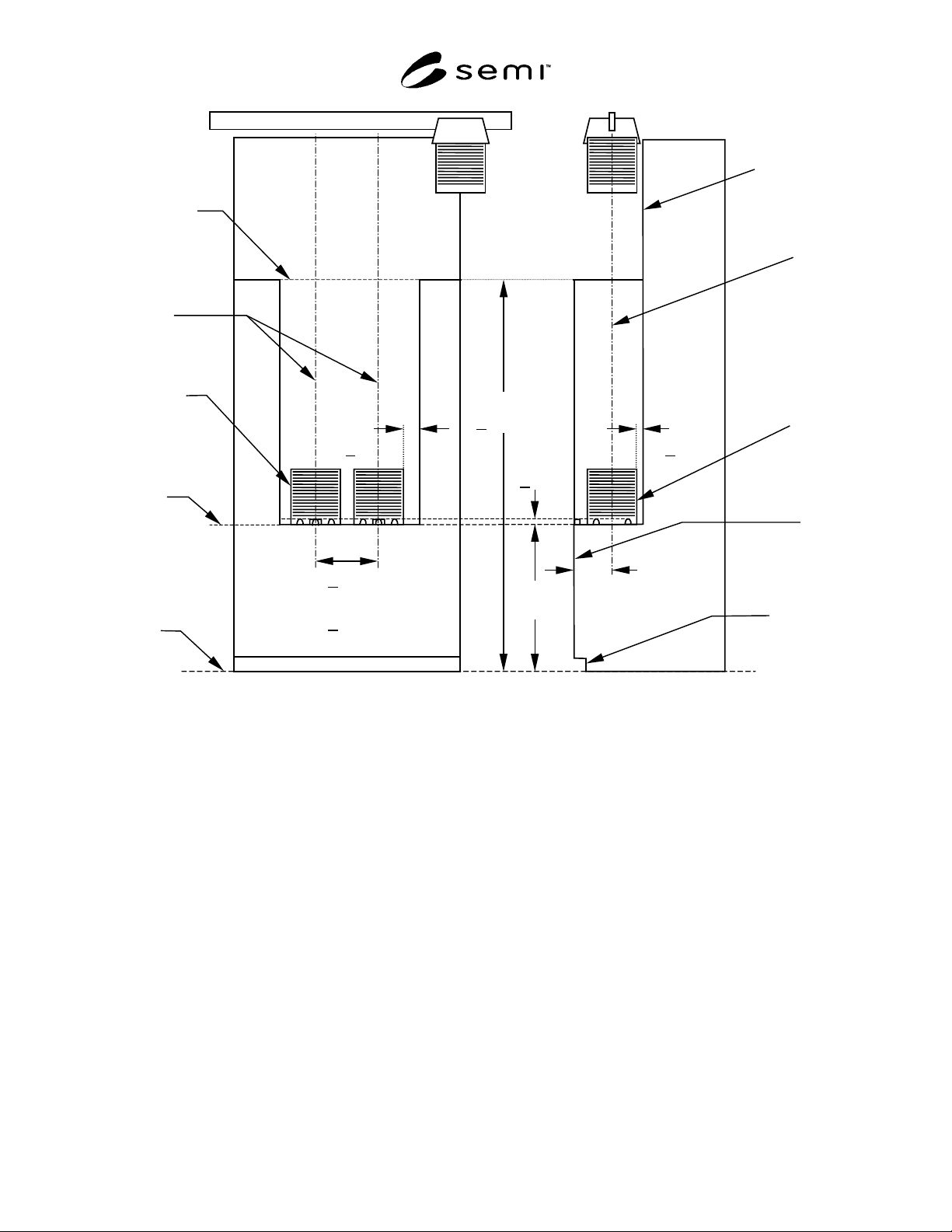
(frame cassette with handles)
equipment
boundar
y
facial
datum
plane
frame
casstte
front
load
face
plane
docking
interface
(see
SEMI E64)
bilateral
datum
planes
frame
cassette
horizontal
datum
plane
floor
H
= 900
H1
< 25
D = 250
C2
> 30
> 482
(frame cassette without handles)
> 555
C1
> 75
+0
–
10
S
H2
< 2600
overhead
track
clearance
Figure 1
Load Port Requirements
SEMI G82-0301
E
© SEMI 2001 5
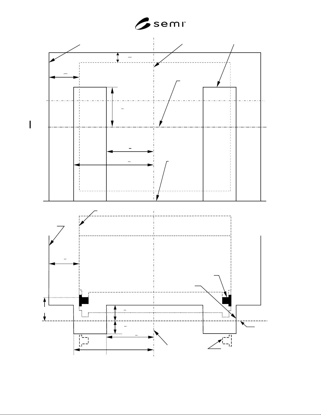
bilateral
datum plane
horizontal
datum plane
H0 > 15
example of conveyor
rail application
conveyor rail is lowered
below fork lift exclusion zone
W1 < 130
W2 > 205
equipment boundary
above H1
frame cassette
C1 > 75
C1 > 75
W1 < 130
W2 > 205
equipment boundary
bilateral
datum plane
facial datum plane
load face plane
D0 > 110
equipment boundary
above H1
equipment boundary
below H1
C2 > 30
H1 < 25
Top
Front
HC3 =32
+2
−
0
Figure 2
Trenches and Conveyor Rails
SEMI G82-0301
E
© SEMI 2001 6
NOTICE: SEMI makes no warranties or representations as to the suitability of the standard set forth herein for any
particular application. The determination of the suitability of the standard is solely the responsibility of the user.
Users are cautioned to refer to manufacturer’s instructions, product labels, product data sheets, and other relevant
literature respecting any materials or equipment mentioned herein. These standards are subject to change without
notice.
The user’s attention is called to the possibility that compliance with this standard may require use of copy-righted
material or of an invention covered by patent rights. By publication of this standard, SEMI takes no position
respecting the validity of any patent rights or copyrights asserted in connection with any item mentioned in this
standard. Users of this standard are expressly advised that determination of any such patent rights or copyrights, and
the risk of infringement of such rights, are entirely their own responsibility.
Copyright by SEMI® (Semiconductor Equipment and Materials
International), 3081 Zanker Road, San Jose, CA 95134. Reproduction o
f
the contents in whole or in part is forbidden without express writte
n
consent of SEMI.