semi合集-English.pdf - 第6114页
SEMI G23-0996 © SE MI 1980, 1996 1 SEMI G23-0996 TEST METHOD FOR INDUCTANCE OF INTERNAL TRACES OF SEMICONDUCTOR P ACKAGES NOTE: This entire docum ent was revised in 1996. 1 Purpose This test method describes the meas ure…

SEMI G22-1296 © SEMI 1980, 19965
Environmental Test
Fine Leak — MIL-STD-883, Method 1014,
Condition B
Gross Leak — MIL-STD-883, Method 1014,
Condition C
Post-Seal Bond Pull
Radiography
Die Shear — MIL-STD-883, Method 2019
Solderability — MIL-STD-883, Method 2003
NOTE 2: An initial vendor qualification may be performed on
the thermal and electrical characteristics of the package. The
characteristics tested will be:
Insulation Resistance — MIL-STD-883, Method 1003,
Test Condition D.
Thermal Dissipation — MIL-STD-883, Method 1012.
12 Packaging and Marking
12.1 Packaging — Containers selected shall be strong
enough and suitably designed to provide maximum
protection against crushing, spillage, and other forms of
damage to the container or its contents to contamination
from exposure to excessive moisture or oxidation by
gases. Packaging materials shall be so selected to
prevent any contamination of the ceramic components
parts with fibers or organic particles.
12.2 Marking — The outer containers shall be clearly
marked identifying the customer part number, customer
purchase order number, drawing number (optional),
quantity, date, and vendor lot number (optional).
NOTICE: These standards do not purport to address
safety issues, if any, associated with their use. It is the
responsibility of the user of these standards to establish
appropriate safety and health practices and determine
the applicability of regulatory limitations prior to use.
SEMI makes no warranties or representations as to the
suitability of the standards set forth herein for any
particular application. The determination of the
suitability of the standard is solely the responsibility of
the user. Users are cautioned to refer to manufacturer’s
instructions, product labels, product data sheets, and
other relevant literature respecting any materials
mentioned herein. These standards are subject to
change without notice.
The user’s attention is called to the possibility that
compliance with this standard may require use of
copyrighted material or of an invention covered by
patent rights. By publication of this standard, SEMI
takes no position respecting the validity of any patent
rights or copyrights asserted in connection with any
item mentioned in this standard. Users of this standard
are expressly advised that determination of any such
patent rights or copyrights, and the risk of infringement
of such rights, are entirely their own responsibility.
Copyright by SEMI® (Semiconductor Equipment and Materials
International), 3081 Zanker Road, San Jose, CA 95134. Reproduction o
f
the contents in whole or in part is forbidden without express written
consent of SEMI.
SEMI G23-0996 © SEMI 1980, 19961
SEMI G23-0996
TEST METHOD FOR INDUCTANCE OF INTERNAL TRACES OF
SEMICONDUCTOR PACKAGES
NOTE: This entire document was revised in 1996.
1 Purpose
This test method describes the measurement method for
the inductance of internal traces of semiconductor
packages.
2 Scope
2.1 This test method is applicable for the measurement
of package inductance that is greater than 0.5 nH.
2.2 This document describes the measurement of a pin
grid array, one of the package types, as a sample.
2.3 This test method is also applic able to other types
of packages.
2.4 The inductance in this docume nt is limited to that
of internal traces only and does not contain the portions
contributed by the exposed areas such as pins and
wires.
2.5 This document uses SI units.
3 Limitation
It is not practical to apply this test method for fine-pitch
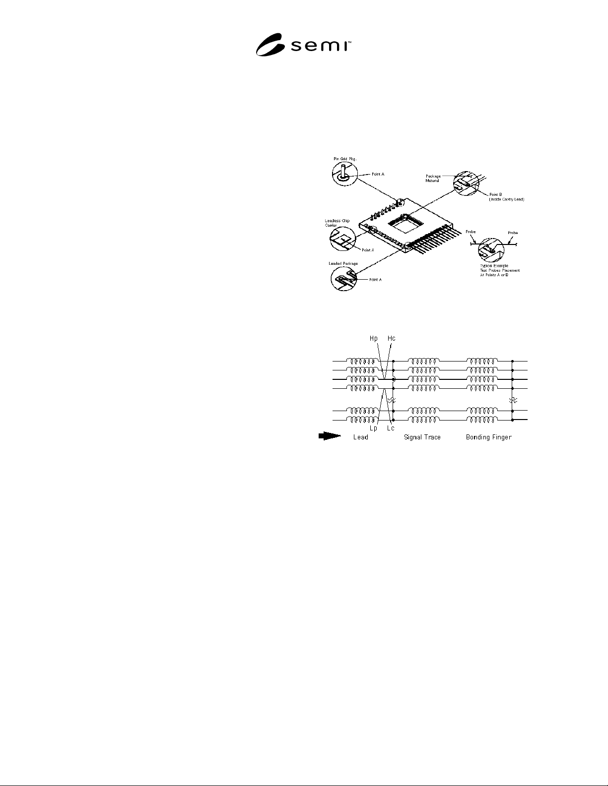
packages where traces or pads (point A of Figure 1)
cannot be connected to with two probes.
4 Referenced Documents
None.
5 Terminology
5.1 internal inductance (of packages) — Inductance of
the circuit that comprises the signal path starts from the
shoulder or in the center of the outside lead (point A of
Figure 1) and ends at the end of the lead on the cavity
side of the lead (point B of Figure 1). The return path is
made by tying all other traces (except for the target
trace in the same electric potential) together. The target
trace is tied to the return path at the bonding finger (see
Figure 2).
Figure 1
Internal Inductance Measurement
Figure 2
Concept of Internal Inductance
5.2 four-point probe — The probe consists of four
coaxial measuring terminals, H
c
(current high), H
p
(potential high), L
c
(current low) and L
p
(potential low),
to measure impedance. Independent coaxial cables are
used between the package being measured and the
measurement instrument to minimize the effect caused
by mutual inductance (between terminals) and/or
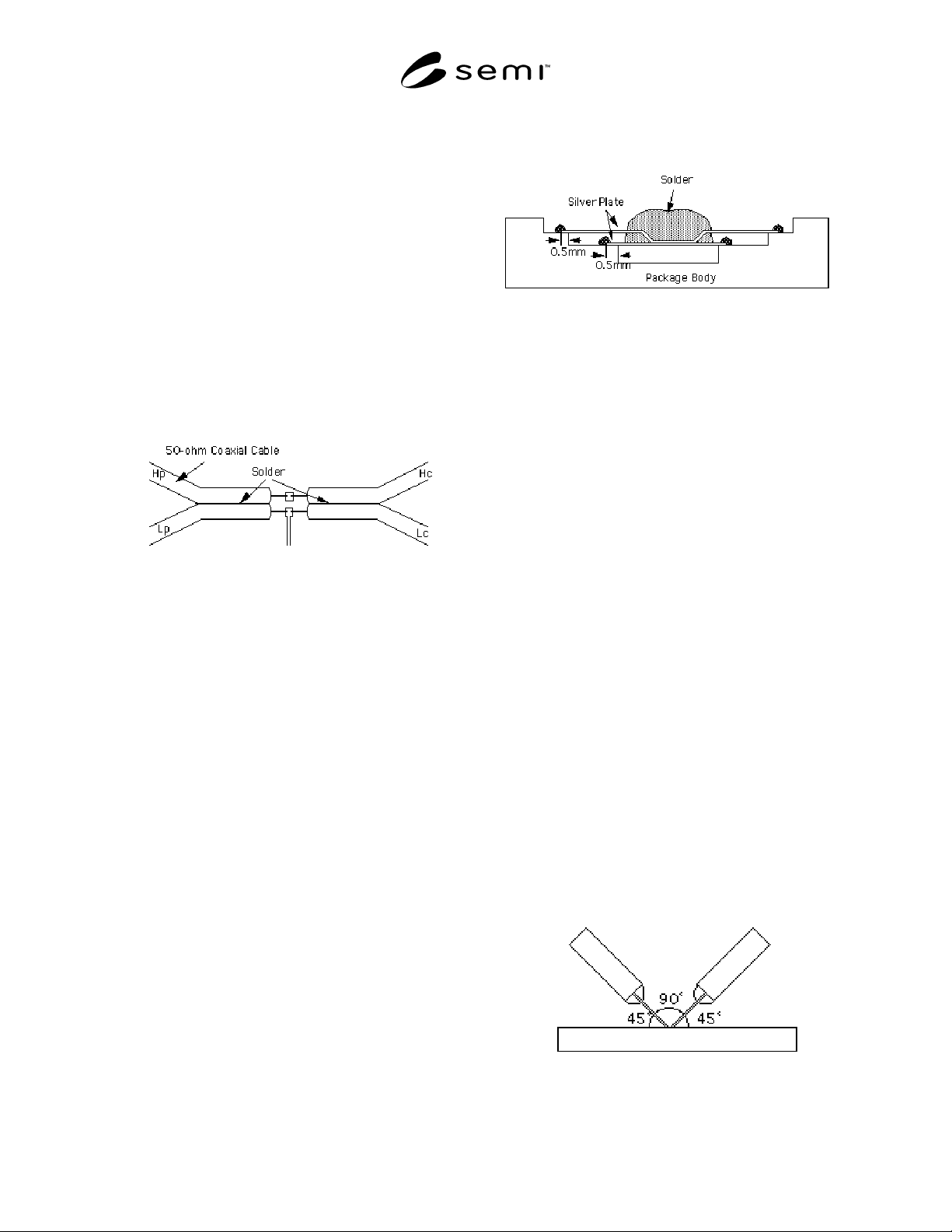
interferences from the measured signals (see Figures 3
and 6).
6 Summary of Method
Fabricate the package to be measured. Then measure
the inductance of internal traces using the four terminal
probe method.
7 Interference
7.1 It is desirable that an operator who is familiar with
the measuring system, measuring method, and
SEMI G23-0996 © SEMI 1980, 1996 2
principles, conduct the actual measurement to get the
best result.
7.2 To get an accurate measurement, maintain equal
probe angle and distance.
8 Apparatus
8.1 LCR Meter
8.1.1 Four terminal probe attachmen t capability
8.1.2 Capable of measuring at the frequency of 10
MHz or higher
8.1.3 Measurement error of less than 0.1 nH for the
measurement range more than 1 nH at the measurement
frequency
8.2 Four Terminal Probe — See F igure 3.
Figure 3
Configuration of Four Terminal Probe
8.2.1 Residual Inductance — less than 1 nH
9 Material
9.1 Copper Plate
9.1.1 Plating — gold
9.1.2 Thickness — 2 mm or thicker
9.2 Insulator — such as Teflon
9.3 Silver Foil
9.3.1 Thickness — around 50 µm
9.4 Solder or Conductive Paste
9.4.1 Resistivity — 10
-4
Ω · m or less
10 Test Specimens
10.1 Preparation of Sample — Conduct the circuit by
measuring the trace as a signal path and the rest, which
has a different potential from this signal path, will be
the return path, as follows:
10.1.1 All the bonding fingers shall b e soldered or
pasted together at the bond finger area to form a short
circuit.
NOTE 1: The short circuit area shall be 0.5 mm from the tip
of the bond fingers. The entire bond fingers shall not be short
circuited (see Figure 4).
Figure 4
Sample Preparation (Part of Bonding Finger)
10.1.2 Short all pins or leads except f or the ones with
the same potential as the trace being measured.
NOTE 2: The location for the short circuit shall be as close as
possible to the bottom of the pins or the braze pad of the leads
to minimize the inductance caused by the pins or leads.
NOTE 3: In case of Pin Grid Array packages, it is
recommended to press 50 µm thickness silver foil, which is
the same size of package, through the pins. In case of Flat
Packages, it is recommended to solder silver foil (or a copper
foil) at the braze pads of the leads.
11 Preparation of Apparatus
Before starting the measurement, warm up the
instruments as specified in the manual.
12 Calibration
Before starting the measurement, calibrate the
instruments as specified in the manual.
13 Procedures
13.1 Measurement of Residual Inductance
13.1.1 Set the LCR meter to the induc tance
measurement mode.
13.1.2 Measure the inductance by conducting the four
terminal probe on the gold plated copper plate as shown
in Figure 5.
Figure 5
Measurement of Residual Inductance