semi合集-English.pdf - 第7569页
SEMI MF1811-0704 © SEMI 2003, 2004 16 Table 4 Values of the Estimates q R ) for Different Types of Detrending Followed by Different Types of W indow ing Type of Data Detrending Type of Window None Piston Piston+Tilt Full…
SEMI MF1811-0704 © SEMI 2003, 2004 15
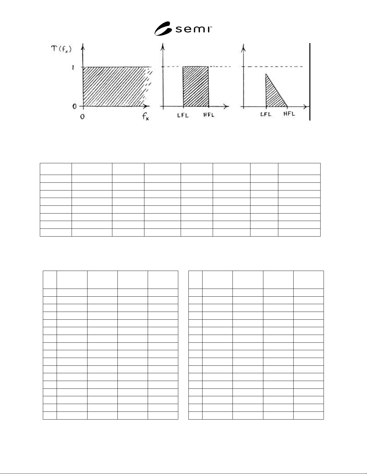
Figure 1
Different Forms of the Measurement-Transfer or Instrumental-Response Function as a Function of Spatial
Frequency, f
x
.
Table 1 Simulated Height Data (N = 32)
n Z(n) n Z(n) n Z(n) n Z(n)
1 –38 9 –40 17 3 25 –35
2 15 10 45 18 6 26 23
3 36 11 20 19 17 27 4
4 22 12 3 20 20 28 –8
5 29 13 47 21 24 29 –45
6 –43 14 –18 22 16 30 26
7 –1 15 45 23 –5 31 1
8 –5 16 43 24 –17 32 6
Table 2 Periodogram Estimates (m)S
)
for Different
Types of Data Detrending Using a Rectangular
Window
m None Piston Piston+Tilt
Full
Quadratic
1 120.0500 0 0 0
2 205.9506 205.9506 182.5409 14.81781
3 142.1861 142.1861 137.3580 204.3631
4 56.98463 56.98463 44.47469 53.08546
5 147.9039 147.9039 139.6268 126.5831
6 58.60630 58.60630 55.67305 50.13899
7 248.4120 248.4120 264.7417 266.1277
8 152.8321 152.8321 158.6038 154.5160
9 185.1250 185.1250 192.8103 190.0105
10 28.81090 28.81090 26.22179 25.40131
11 28.61438 28.61438 27.90264 28.74841
12 153.1641 153.1641 145.7812 145.2367
13 356.5711 356.5711 366.4113 365.4717
14 199.1965 199.1965 202.6268 203.4514
15 41.53757 41.53757 40.26207 40.50671
16 163.6550 163.6550 168.8428 169.0258
17 16.20000 16.20000 17.87214 17.87215
Table 3 Periodogram Estimates (m)S
)
for Different
Types of Data Detrending Using a Blackman
Window
m None Piston Piston+Tilt
Full
Quadratic
1 312.4632 87.20874 90.11245 9.832211
2 536.6033 268.4217 260.2453 76.63136
3 195.1412 166.9871 162.0176 93.70938
4 1.046170 1.046172 1.041742 1.303189
5 30.14155 30.14156 30.16028 30.25176
6 54.87353 54.87350 54.91950 54.94658
7 188.9816 188.9818 188.8795 188.8293
8 74.45938 74.45934 74.50156 74.51955
9 45.28967 45.28967 45.27541 45.29324
10 59.40473 59.40471 59.41950 59.41210
11 94.24771 94.24768 94.23248 94.23342
12 202.7328 202.7328 202.7405 202.7253
13 289.7414 289.7414 289.7450 289.7637
14 130.1287 130.1287 130.1230 130.1162
15 76.22277 76.22275 76.22527 76.22248
16 62.42836 62.42840 62.42742 62.43071
17 5.585947 5.585948 5.585947 5.584926
SEMI MF1811-0704 © SEMI 2003, 2004 16
Table 4 Values of the Estimates
q
R
)
for Different Types of Detrending
Followed by Different Types of Windowing
Type of Data Detrending
Type of Window
None Piston Piston+Tilt Full Quadratic
Rectangular 26.13517 26.13517 26.05133 25.34362
Hann 25.49031 24.02299 23.91725 22.31003
Hamming 25.53997 24.26072 24.15406 22.58759
Blackman 25.29220 23.38999 23.30221 21.54917
NOTICE: SEMI makes no warranties or representations as to the suitability of the standards set forth herein
for any particular application. The determination of the suitability of the standard is solely the responsibility of
the user. Users are cautioned to refer to manufacturer' s instructions, product labels, product data sheets, and
other relevant literature, respecting any materials or equipment mentioned herein. These standards are subject
to change without notice.
By publication of this standard, Semiconductor Equipment and Materials International (SEMI) takes no
position respecting the validity of any patent rights or copyrights asserted in connection with any items
mentioned in this standard. Users of this standard are expressly advised that determination of any such patent
rights or copyrights, and the risk of infringement of such rights are entirely their own responsibility.
Copyright by SEMI® (Semiconductor Equipment and Materials
International), 3081 Zanker Road, San Jose, CA 95134. Reproduction o
f
the contents in whole or in part is forbidden without express written
consent of SEMI.

SEMI MF1982-1103 © SEMI 2003 1
SEMI MF1982-1103
TEST METHODS FOR ANALYZING ORGANIC CONTAMINANTS ON
SILICON WAFER SURFACES BY THERMAL DESORPTION GAS
CHROMATOGRAPHY
This standard was technically approved by the Global Silicon Wafer Committee and is the direct
responsibility of the North American Silicon Wafer Committee. Current edition approved for publication by
the North American Regional Standards Committee on July 27, 2003. Initially available at www.semi.org
October 2003; to be published November 2003. Originally published by ASTM International as ASTM
F 1982-99. Last previous edition ASTM F 1982-99
ε1
.
1 Purpose
1.1 Organics are present in many materials, such as
plastics, lubricants, cleansers, soaps, and living tissues.
Some of these compounds are volatile and others can
become airborne through chemical reactions, heating,
abrasion, or outgassing. Also they can transfer to
wafers by direct contact or be left behind from solvent
residues. Once present in clean facilities, they can
deposit on wafer surfaces. Organics deposited on
wafers can cause degradation haze, wafer surface
tension changes, irregular oxidation rates, and other
effects, such as counter-doping by organophosphorus
compounds. Identification of trace level organic
contaminants is important in determining the source of
the particular contamination. These test methods use
the TD-GC technique to characterize and quantify
organics deposited on wafer surfaces.
1.2 Monitoring of organic contamination on wafer
surfaces also can be used to measure material
outgassing for proper selection of cleanroom,
construction, and wafer packaging materials.
2 Scope
2.1 These test methods cover the identification and
quantification of organic contaminants on silicon wafer
surfaces using a gas chromatograph interfaced to a mass
spectrometer (GC-MS) or a phosphorus selective
detector, or both.
2.2 These test methods describe the apparatus and
related procedures for sample preparation and analyses
by thermal desorption gas chromatography (TD-GC).
1
,
2
2.3 The range of detection limits of these test methods
depends on the target organic compounds, for example,
the range of detection limits is from the subpicogram to
the nanogram level of hydrocarbons (C
8
to C
28
) per
square centimeter of silicon wafer surface.
1 Fergason, L.A., “Analysis of Organic Impurities on Silicon Wafer
Surfaces,” Microcontamination, 4(4), 33-37, April 1986.
2 Saga, K. and Hattori, T., “Identification and Removal of Trace
Organic Contamination on Silicon Wafers Stored in Plastic Boxes,”
Journal of Electrochemical Society, 143, 3270-3284 (1996).
2.4 These test methods can be used for polished silicon
wafers, or silicon wafers with oxide films.
2.5 Two methods are described. Method A is
performed on cleaved wafers. Method B is performed
on full wafers. The detailed procedures of Method A
and Method B as well as the differences between them,
are described in Sections 5 and 7 .
2.6 Suitable safety precautions must be followed when
handling organic solvents and compounds, hot
materials subjected to propane flame, the propane flame
itself, wafer thermal desorption systems, rapid thermal
annealer, or a high temperature furnace.
NOTICE: This standard does not purport to address
safety issues, if any, associated with its use. It is the
responsibility of the user of this standard to establish
appropriate safety and health practices and determine
the applicability of regulatory or other limitations prior
to use.
3 Referenced Standards
3.1 ASTM Standard
D 6196 — Practice for Selection of Sorbents and
Pumped Sampling/Thermal Desorption Analysis
Procedures for Volatile Organic Compounds in Air
3
NOTICE: Unless otherwise indicated, all documents
cited shall be the latest published versions.
4 Terminology
4.1 Abbreviations and Acronyms
4.1.1 AED — atomic emission detector
4.1.2 C
16
— n-hexadecane, n-C
16
H
34
4.1.3 FID — flame ionization detector
4.1.4 FPD — flame photometric detector
4.1.5 GC — gas chromatography
3 Published in Volume 11.03 of Annual Book of ASTM Standards.
Available from ASTM International, 100 Barr Harbor Drive, West
Conshohoken, PA 19428-2959, USA. Telephone: 610.832.9585,
Fax: 610.832-9555, Web site:
www.astm.org
.