semi合集-English.pdf - 第174页
SEMI E22-0697 © SEMI 1991, 2002 1 SEMI E22-0697 (Reapproved 1102) CLUSTER TOOL MODULE INTERF ACE: TRANSPOR T MODULE END EFFECTOR EXCLUSION VOLUME STANDARD This standard was technically rea pproved by the Global Physical …

SEMI E21.1-1296 © SEMI 1992, 2002 5
RELATED INFORMATION 1
NOTE: The material contained in this related information is not an official part of SEMI E21.1, and is not meant to
modify or supersede it in any way. Rather, these notes are provided primarily as a source of information to aid in the
application of the standard. As such they are to be considered as reference material only. The standard should be
referred to in all cases.
R1-1 Vertical Requirements
R1-1.1 Changes in vertical requirements are made because of the need to provide adequate transport arm stiffness
(thickness) for the longer reach specified for 300 mm. However, for many processes, it is desirable to limit the slot
size as far as possible. An option is now allowed to reduce the vertical slot opening on the Attached Modules side of
the Interface Plane (see Figure 1, E21), but any such reduction will compromise the space otherwise available for
transport arm vertical thickness and/or movement. Specification of the extent of this option will be needed in each
case it is used.
R1-2 Transport Maximum Reach
A1-2.1 The maximum reach beyond the interface plane (see Table 1) is increased by 75 mm (from 305.0 mm to
380.0 mm); a 50 mm increase in wafer radius (from 100 mm to 150 mm) and a 25 mm increase in clearance between
the wafer and the chamber walls.
R1-3 Width Requirements
R1-3.1 The increase in wafer diameter from 200 mm to 300 mm necessitates a 100 mm increase in all width values
(see Table 1) specified in SEMI E21.
NOTICE: SEMI makes no warranties or representations as to the suitability of the standards set forth herein for any
particular application. The determination of the suitability of the standard is solely the responsibility of the user.
Users are cautioned to refer to manufacturer' s instructions, product labels, product data sheets, and other relevant
literature, respecting any materials or equipment mentioned herein. These standards are subject to change without
notice.
The user’s attention is called to the possibility that compliance with this standard may require use of an invention
covered by patent rights. By publication of this standard, Semiconductor Equipment and Materials International
(SEMI) takes no position respecting the validity of any patent rights asserted in connection with any item mentioned
in this standard. In particular, users of the specification should be aware that Drytek, Inc., A Unit of General Signal,
16 Jonspin Road, Wilmington, MA 01887-1087, Phone: (508) 657-3933, has neither claimed nor disclaimed that
compliance with this specification would require use of an invention covered by one or more of its patents. Users of
this standard are expressly advised that determination of any such patent rights, and the risk of the infringement of
such rights, are entirely their own responsibility.
Copyright by SEMI® (Semiconductor Equipment and Materials
International), 3081 Zanker Road, San Jose, CA 95134. Reproduction o
f
the contents in whole or in part is forbidden without express written
consent of SEMI.

SEMI E22-0697 © SEMI 1991, 2002 1
SEMI E22-0697 (Reapproved 1102)
CLUSTER TOOL MODULE INTERFACE: TRANSPORT MODULE END
EFFECTOR EXCLUSION VOLUME STANDARD
This standard was technically reapproved by the Global Physical Interfaces & Carriers Committee and is the
direct responsibility of the North American Physical Interfaces & Carriers Committee. Current edition
reapproved by the North American Regional Standards Committee on July 21, 2002. Initially available at
www.semi.org October 2002; to be published November 2002. Originally published in 1991; previously
published June 1997.
1 Purpose
1.1 The purpose of the standard is to provide sufficient
detail to allow the transport module end effector to
move wafers to and from process and cassette modules
in a cluster tool without mechanical interference.
2 Scope
2.1 The standard describes the volume within any
process or cassette module which shall be accessible to
the transport module end effector in a cluster tool. The
standard is limited to modules which accommodate
wafer sizes from 100 mm up to and including 200 mm
in diameter.
2.2 This standard does not purport to address safety
issues, if any, associated with its use. It is the
responsibility of the users of this standard to establish
appropriate safety health practices and determine the
applicability or regulatory limitations prior to use.
3 Impact
3.1 The adoption of the standard requires equipment
designers to allow specific unobstructed volumes within
process and cassette modules for wafer transport and
places restrictions on the design of the transport module
end effector. Some restrictions are dependent on the
wafer size.
4 Referenced Standards
4.1 SEMI Standards
SEMI E1 — Specification for 3 inch, 100 mm, 125
mm, and 150 mm Plastic and Metal Wafer Carriers
SEMI E21 — Cluster Tool Module Interface:
Mechanical Interface and Wafer Transport Standard
5 Terminology
5.1 Definitions
5.1.1 exclusion zone — A restricted area within a
process or cassette module reserved for access by the
transport module end effector during wafer handling.
5.1.2 fork — A two-prong transport module end
effector designed to hold the wafer around its
periphery.
5.1.3 paddle — A blade transport module end effector
designed to support the wafer.
5.1.4 pedestal — A support pillar axially symmetric to
the wafer transport position in a process or cassette
module.
5.1.5 slot — A two-sided support, for example as
defined for a standard wafer carrier in SEMI E1 when
the carrier is oriented with its axis in a vertical attitude.
5.1.6 transport module end effector — That part of the
transport module that supports the wafer and can extend
beyond the interface plane (defined in SEMI E21).
5.1.7 wafer support platform — A slot, pedestal, or set
of pins used to hold a wafer in a horizontal attitude.
5.1.8 wafer transport axis — The centerline of
transport module end effector motion. This centerline is
symmetric with the wafer transport zone as described in
SEMI E21.
5.1.9 wafer transport position — A location within a
process or cassette module where the wafer is accepted
or presented by the transport module end effector. This
is also the location of the wafer centroid.
6 Requirements
6.1 Wafer Transport — The wafer is to be transported
in a horizontal attitude (see Related Information R1-1).
6.2 Wafer Transport Plane Exclusion Zone — The
exclusion zone is illustrated in Figure 1, and the
variables are defined in Table 1 and specified in Table 2
(see Related Information R1-2). The clear areas
between B and C and along the wafer transport axis are
specified to allow the transport module end effector to
be retracted after the wafer has been placed on the
support platform in the process or cassette module. The
right-hatched (////) area denotes the exclusion zone
which could be occupied by a paddle. The left-hatched
(\ \ \ \ ) area denotes the additional exclusion zone which
could be occupied by a fork. The cross-hatched
(XXXX) area denotes the reduction in the dimensions
SEMI E22-0697 © SEMI 1991, 2002 2
of the paddle exclusion zone to accommodate a pedestal
and or pin(s) in a process or cassette module (referred
to as a pedestal or pin exclusion zone).
6.3 Maximum Pedestal Diameter — The diameter is
not to exceed dimension H given in Table 2.
6.4 Pin Location — Wafer support pins to be located
relative to the wafer transport plane exclusion zone.
The pins are to be located at radii dependent upon wafer
diameter as specified in Table 2.
6.5 Vertical Plane Exclusion Zone — The extent of the
exclusion zone in the vertical plane is indicated by the
hatched area and the dashed outline in Figure 2. The
maximum extent of the exclusion zone allows the
transport module end effector to clear the minimum
wafer transport zone at the interface plane (see Related
Information R1-3). The vertical plane exclusion zone is
decreased in height in the vicinity of the wafer transport
position to allow the presence of shields, electrodes,
etc. in the process or cassette module.
6.6 Transport Module End Effector Exclusion Volume
— The exclusion volume within a process or cassette
module reserved for access by the transport module end
effector is defined by the intersection of the two
orthogonal exclusion zones described in Sections 6.2
and 6.5. This exclusion volume allows the transport
module end effector to accept or present a wafer at the
wafer transport position within a process or cassette
module (see Related Information R1-4).
LIST OF FIGURES
Figure 1. Wafer Transport Plane Exclusion Zone (Plan
View)
Figure 2. Vertical Plane Exclusion Zone (Elevation
View)
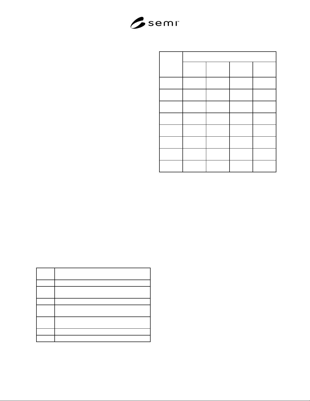
Table 1 Wafer Transport Plane Exclusion Zone
Variables
A Maximum width of the wafer transport plane
exclusion zone
B Minimum outside clearance for support pins
C Maximum inside clearance for support pins
and/or slot
D Minimum radial clearance for support pins
E Outermost radius of wafer transport plane
exclusion zone
F Minimum clearance for entry into SEMI
Standard Wafer Carrier
G Maximum clearance for support pins
H Maximum clearance for support pedestal
Table 2 Wafer Transport Plane Exclusion Zone
Dimensions
Wafer Size
Variables
100 mm
(4 in.)
125 mm
(5 in.)
150 mm
(6 in.)
200 mm
(8 in.)
A 120 mm
(4.72 in.)
145 mm
(5.71 in.)
170 mm
(6.69 in.)
220 mm
(8.66 in.)
B 86 mm
(3.39 in.)
107 mm
(4.21 in.)
129 mm
(5.08 in.)
172 mm
(6.77 in.)
C 50 mm
(1.97 in.)
66 mm
(2.60 in.)
78 mm
(3.07 in.)
104 mm
(4.09 in.)
D 47 mm
(1.85 in.)
60 mm
(2.36 in.)
72 mm
(2.83 in.)
97 mm
(3.82 in.)
E 60 mm
(2.36 in.)
72 mm
(2.83 in.)
85 mm
(3.35 in.)
110 mm
(4.33 in.)
F 70 mm
(2.76 in.)
82 mm
(3.23 in.)
95 mm
(3.74 in.)
120 mm
(4.72 in.)
G 47 mm
(1.85 in.)
60 mm
(2.36 in.)
72 mm
(2.83 in.)
97 mm
(3.82 in.)
H 30 mm
(1.18 in.)
38 mm
(1.50 in.)
45 mm
(1.77 in.)
60 mm
(2.36 in.)