semi合集-English.pdf - 第7580页
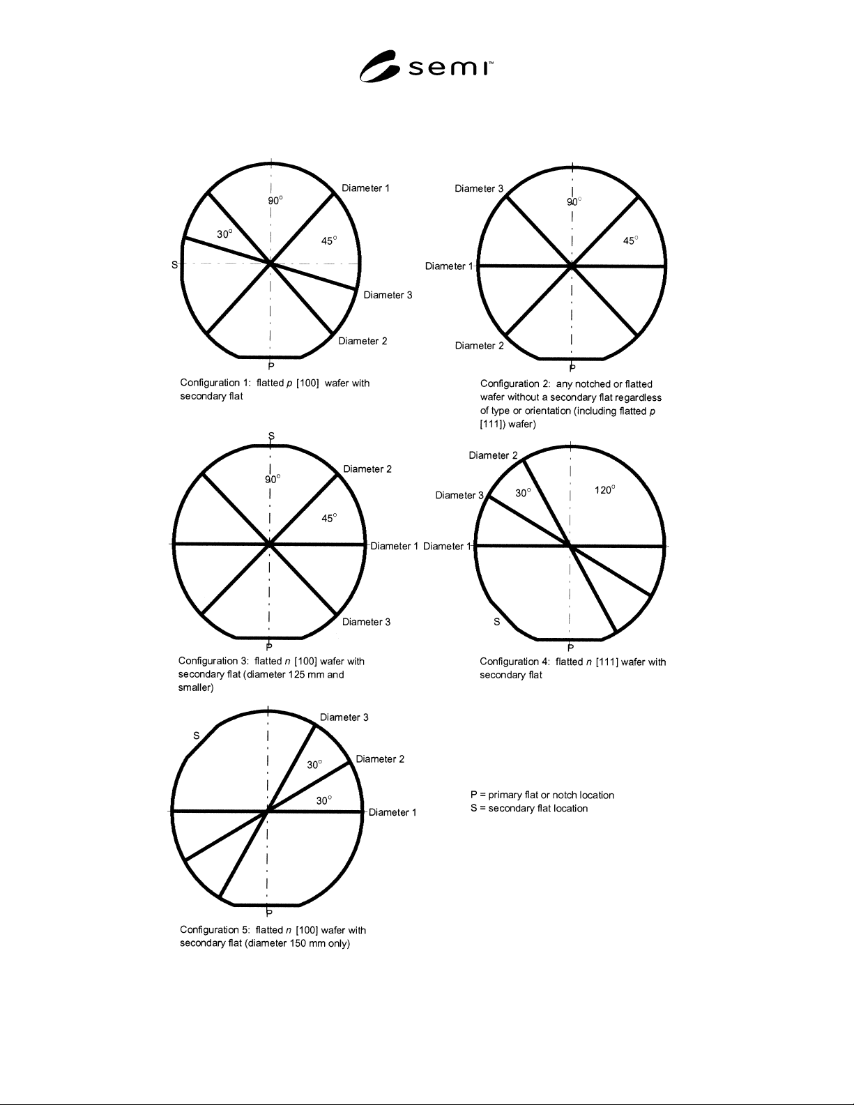
SEMI MF2074-1103 © SEMI 2003 3 Table 1 Positions for Measuremen t of Wafer Diameter Configuration Primary Fiducia l Secondary Fl at Diameter 1 Diameter 2 Diameter 3 1 270° 180° 45° 135° 165° 2 270° none 0° 45° 135° 3 270…
SEMI MF2074-1103 © SEMI 2003 2
7 Keywords
7.1 diameter, semiconductor, silicon, wafer
Figure 1
Diameter Measurement Positions by Wafer Fiducials Category
SEMI MF2074-1103 © SEMI 2003 3
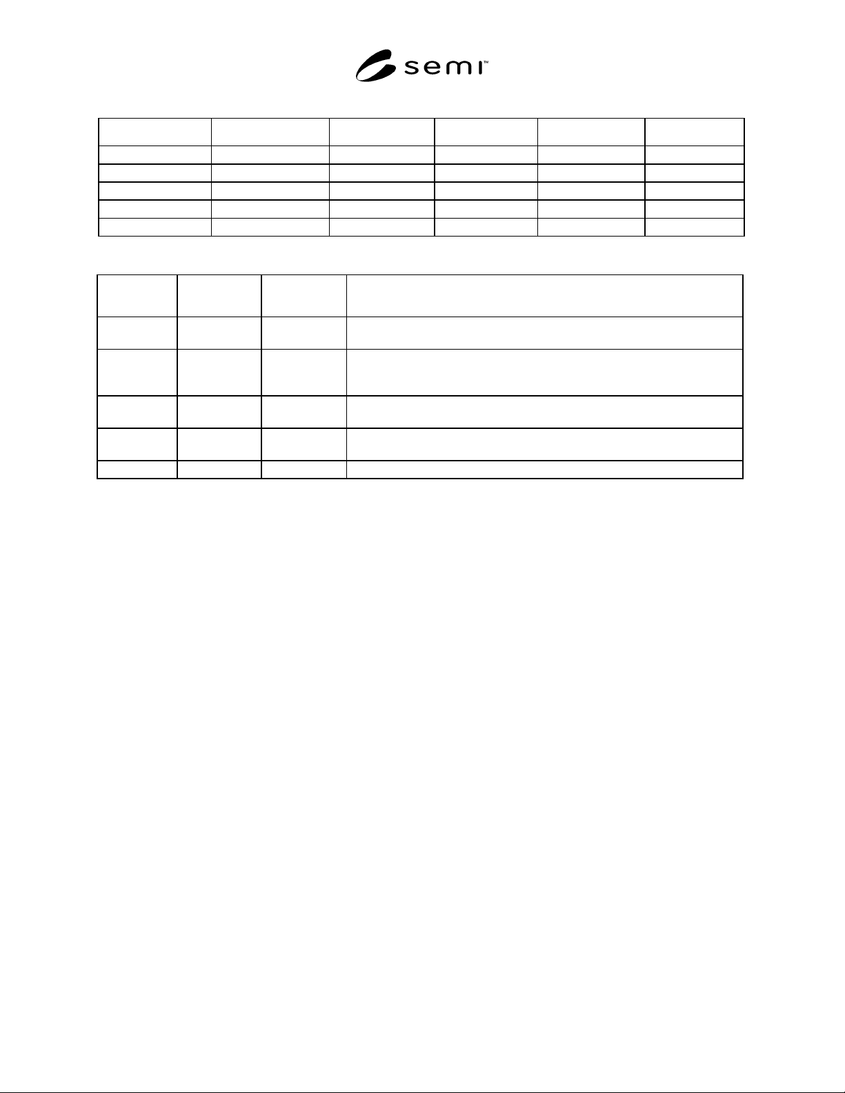
Table 1 Positions for Measurement of Wafer Diameter
Configuration Primary Fiducial Secondary Flat Diameter 1 Diameter 2 Diameter 3
1 270° 180° 45° 135° 165°
2 270° none 0° 45° 135°
3 270° 90° 0° 45° 135°
4 270° 225° 0° 120° 150°
5 270° 135° 0° 30° 60°
Table 2 Wafer Types and Orientations Corresponding to Measurement Configuration of Table 1
Configuration
Conductivity
Type
Orientation Notes
1 p [100] Applies only to [100] p-type wafers, 150 mm and smaller, with secondary
flats
2 p [111] Applies both to [111] p-type wafers, 150 mm and smaller, (without
secondary flats) and to all other notched and flatted wafers without secondary
flats regardless of conductivity type and orientation
3 n [100] Applies only to [100] n-type wafers, 125 mm and smaller, with secondary
flats
4 n [111] Applies only to [111] n-type wafers, 150 mm and smaller, with secondary
flats
5 n [100] Applies only to [100] n-type 150 mm wafers with secondary flats
NOTICE: SEMI makes no warranties or representations as to the suitability of the standards set forth herein for any
particular application. The determination of the suitability of the standard is solely the responsibility of the user.
Users are cautioned to refer to manufacturer' s instructions, product labels, product data sheets, and other relevant
literature, respecting any materials or equipment mentioned herein. These standards are subject to change without
notice.
By publication of this standard, Semiconductor Equipment and Materials International (SEMI) takes no position
respecting the validity of any patent rights or copyrights asserted in connection with any items mentioned in this
standard. Users of this standard are expressly advised that determination of any such patent rights or copyrights, and
the risk of infringement of such rights are entirely their own responsibility.
Copyright by SEMI® (Semiconductor Equipment and Materials
International), 3081 Zanker Road, San Jose, CA 95134. Reproduction o
f
the contents in whole or in part is forbidden without express written
consent of SEMI.

SEMI MF2139-1103 © SEMI 2003 1
SEMI MF2139-1103
TEST METHOD FOR MEASURING NITROGEN CONCENTRATION IN
SILICON SUBSTRATES BY SECONDARY ION MASS SPECTROMETRY
This standard was technically approved by the Global Silicon Wafer Committee and is the direct
responsibility of the North American Silicon Wafer Committee. Current edition approved for publication by
the North American Regional Standards Committee on July 27, 2003. Initially available at www.semi.org
October 2003; to be published November 2003. Originally published by ASTM International as ASTM
F 2139-01. Last previous edition ASTM F 2139-01.
1 Purpose
1.1 Secondary ion mass spectrometry (SIMS) can
measure in un-annealed, polished Czochralski (CZ)
silicon substrates the nitrogen concentration that may
be intentionally introduced to: (1) increase the V/G
tolerance for grown-in defects free region, where V is
the pull rate and G is the crystal temperature gradient at
the solid-liquid interface;
1
(2) increase the void-free
denuded zone depth and the bulk micro-defect density
after annealing in hydrogen or argon;
2,3
(3) reduce the
crystal originated particle (COP) size after annealing;
2,3
or (4) enhance the precipitation of oxygen in epitaxial
substrates under reduced temperature processing.
4
1.2 SIMS can measure total bulk nitrogen in CZ-
silicon, whereas infrared spectroscopy is negatively
affected by the chemical state in oxygen-containing
silicon.
5
In addition, SIMS can measure the total bulk
nitrogen in p
+
(B) and n
+
(Sb) substrates used for
epitaxial silicon, whereas infrared spectroscopy cannot
due to free electron absorption interferences.
1.3 SIMS can measure in un-annealed, polished Float-
zoned (FZ) silicon substrates the nitrogen concentration
1 Iida, M., Kusaki, W., Tamatsuka, M., Iino, E., Kimura, M., and
Muraoka, S., “Effects of Light Element Impurities on the Formation
Grown-In Defects Free Region of Czochralski Silicon Single
Crystal,” in Defects in Silicon III, edited by W. M. Bullis, W. Lin, P.
Wagner, T.Abe, and S. Kobayashi, The Electrochemical Society
Proceedings Series PV99-1 (The Electrochemical Society,
Pennington, NJ, 1999) pp. 499-510.
2 Tamatsuka, M., Kobayashi, N., Tobe, S., and Masui, T., “High
Performance Silicon Wafer with Wide Grown-in Void Free Zone and
High Density Internal Gettering Site Achieved via Rapid Crystal
Growth with Nitrogen Doping and High Temperature Hydrogen
and/or Argon Annealing,” ibid., pp.456-467.
3 Minami, T., Takeda, R., Saito, H., Hirano, Y., Suzuki, O., Nitta, S.
Kashima, K., and Matsushita, Y., “Influence of Void Size on the
Formation of Defect Free Regions in Hydrogen Annealed CZ Silicon
Wafers,” ECS Extended Abstract No.514, 197th Meeting of the
Electrochemical Society, (The Electrochemical Society, Pennington,
NJ, 2000).
4 Shimura, F., and Hockett, R. S., “Nitrogen effect on oxygen
precipitation in Czochralski silicon,” Appl. Phys. Lett. 48, 224-226
(1986).
5 Abe, T., Kikuchi, K., Shirai, S., and Muraoka, M., in Semicon-
ductor Silicon 1981, edited by H. R. Huff, R. J. Kriegler and Y.
Takeishi, (The Electrochemical Society, Pennington, NJ, 1981) pp.
54-71.
that may be introduced to strengthen low oxygen
substrates.
1.4 The SIMS method can be used for process check of
crystal doping, and for research and development.
2 Scope
2.1 This test method covers the determination of total
nitrogen concentration in the bulk of single crystal
substrates using secondary ion mass spectrometry
(SIMS).
6,7
2.2 This test method can be used for silicon in which
the dopant concentrations are less than 0.2% (1 × 10
20
atoms/cm
3
) for boron, antimony, arsenic, and
phosphorus.
2.3 This test method is for bulk analysis where the
nitrogen concentration is constant with depth.
2.4 This test method can be used for silicon in which
the nitrogen content is 1 × 10
14
atoms/cm
3
or greater.
The detection capability depends upon the SIMS
instrumental nitrogen background and the precision of
the measurement.
2.5 This test method is complementary to infrared
spectroscopy, electron paramagnetic resonance, deep
level transient spectroscopy, and charged particle
activation analysis.
8
The infrared spectroscopy method
detects nitrogen in specific vibrational states, rather
than total nitrogen, and is limited to silicon with doping
concentrations less than about 1 × 10
17
atoms/cm
3
. The
6 Hockett, R. S., Evans, Jr., C. A., and Chu, P. K., “The SIMS
Measurement of Nitrogen in Nitrogen-Doped CZ-Silicon,” in
Secondary Ion Mass Spectrometry SIMS VI, edited by A.
Benninghoven, A. M. Huber, and H. W. Huber, (John Wiley & Sons,
New York, 1988) pp. 441-444.
7 Hockett, R. S. and Sams, D. B., “The Measurement of Nitrogen in
Silicon Substrates by SIMS,” in High Purity Silicon VI, edited by C.
L. Claeys, P. Rai-Choudhury, M. Watanabe, P. Stallhofer, and H. J.
Dawson, ECS Proceedings Vol PV 2000-17 (The Electrochemical
Society, Pennington, NJ, 2000) pp. 584-595.
8 Stein, Herman J., “Nitrogen in Crystalline Si,” in Materials
Research Society Symposia Proceedings Vol 59, Oxygen, Carbon,
Hydrogen and Nitrogen in Crystalline Silicon, edited by J. C.
Mikkelsen, Jr., S. J. Pearton, J. W. Corbett, and S. J. Pennycook,
(Materials Research Society, Pittsburgh, PA, 1986) pp. 523-535.