semi合集-English.pdf - 第5314页
SEMI M49-0704 © SEMI 2001, 2004 13 APPENDIX 1 SCALING MODELS NOTICE : The material in this appendix is an official part of SEMI M49 and was approved by fu ll letter ballot procedures on May 14, 2004. Table A1-1 Scaling m…
SEMI M49-0704 © SEMI 2001, 2004 12
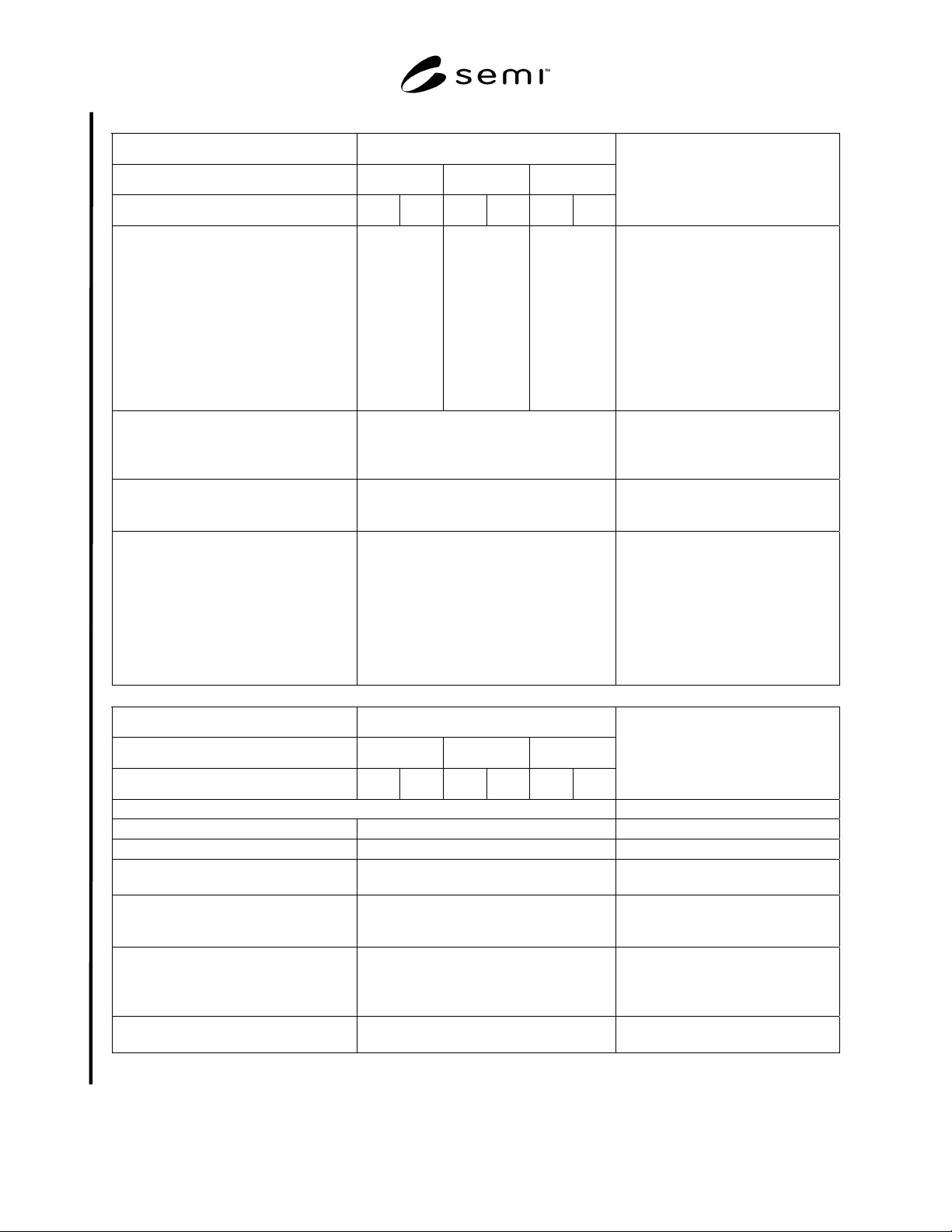
3. SETUP PARAMETERS
Item Recommended Specification
Technology Generation 130 nm 90 nm 65 nm
Grade A B A B A B
Comments and References
3.1 Nominal Edge Exclusion defining
FQA (mm)
≥ 2
≥
≥ 1
Performance parameters are to be
verified with nominal edge exclusion
≥ 2 mm. Instrument must be capable
of reporting to nominal edge
exclusion ≥ 1 mm. As a guide, the
extended performance for nominal
edge exclusion < 2 mm should not
exceed the performance (σ
3
,
matching, bias) by more than 100 %
as compared to ≥2 mm edge exclusion
given appropriate reference material.
3.2 Site Patterns For local flatness: use any site pattern
compatible with SEMI M1; for
nanotopography use floating sites
Recommended range for site size: 5 –
40 mm, arbitrary combination of
length of rectangular sides; see SEMI
M1, SEMI M43
3.3 Sorting Criteria Sorting is performed by using logical
“AND/OR” combinations of multiple
parameters
3.4 Exclusion Windows a) > 3, curved or linear boundaries with
arbitrary position anywhere on the
entire wafer surface
b) perimeter exclusion windows: N zones
with total area covered ≤ 0.001 of total
wafer area in the range R – 2 mm to R,
total perimeter excluded at R – 1 mm
≤ 4% of total wafer circumference, no
single zone longer than 5 mm.
a) e.g., laser mark exclusion
4. PERFORMANCE
Item Recommended Specification
Technology Generation 130 nm 90 nm 65 nm
Grade A B A B A B
Comments and References
4.1 Throughput
4.1.1 200 mm Wafers > 60 wafers per hour
4.1.2 300 mm Wafers > 40 wafers per hour
4.2 Downward Compatibility At least one previous tool generation of
supplier
Specific tools involved need to be
identified
4.3 Calibration Automated method, Certified Reference
Material (CRM) to be provided by
equipment supplier.
4.3.1 Level 3 Variability Test Interval
≥ 10 measurements over a period of not less
than 2 weeks (See NOTE 1.)
To be performed with throughput
mode used for qualifying product
wafers, 95% confidence interval has
to be less than the specified σ
3
4.4 Dependence of Results on Wafer
Orientation
< 1 σ
3
NOTE 1: This recommended specification is not intended to be a requirement for a two week pre-shipment test. Performance could be verified
through routine SPC (Statistical Process Control).
SEMI M49-0704 © SEMI 2001, 2004
13
APPENDIX 1
SCALING MODELS
NOTICE: The material in this appendix is an official part of SEMI M49 and was approved by full letter ballot procedures on
May 14, 2004.
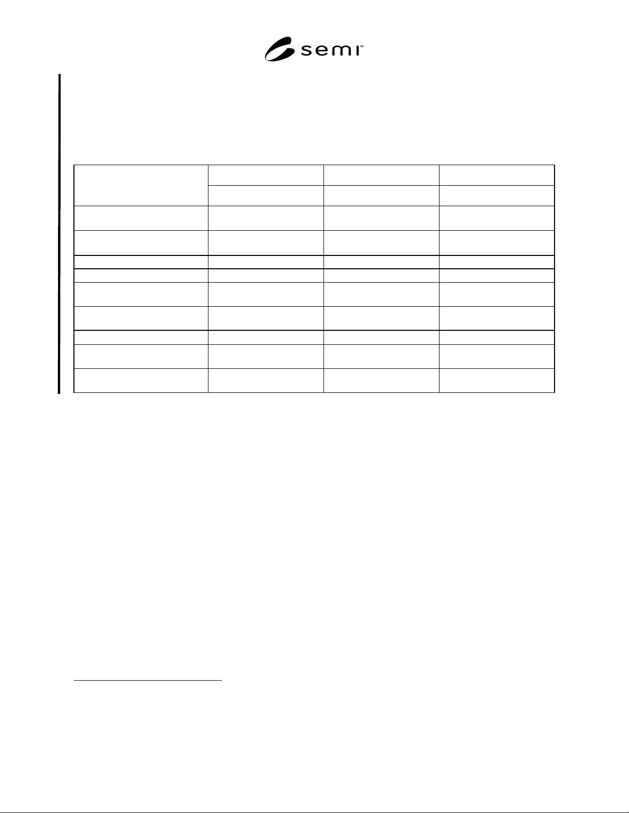
Table A1-1 Scaling models used in Tab. 3.1 for the technology nodes 130 to 65 nm
130 nm node 90 nm node 65 nm node
Property
nominal nominal nominal
1.1 Thickness (200 mm wafers),
µm
725 no scaling no scaling
1.2 Thickness (300 mm wafers),
µm
775 no scaling no scaling
1.3 GBIR, nm 1000 no scaling no scaling
1.4 Site Size local flatness, mm
2
25*25 26*8 26*8
1.4.1 SBIR, including
partial sites, nm
250
2/3 of (120 nm + max. SFQR
per ITRS)
10
2/3 of (120 nm + max. SFQR
per ITRS)
10
1.4.2 SFQR, including
partial sites, nm
130
2/3 of max value acc. to
ITRS
11
2/3 of max value acc. to
ITRS
11
1.5 Warp, µm
30 no scaling no scaling
1.6 Nanotopography, 2 mm, P-V,
nm, at 0.05% defective area
20
2/3 of max value acc. to
ITRS
11
2/3 of max value acc. to
ITRS
11
1.7 Nanotopography, 10 mm, P-V,
nm, at 0.05% defective area
70 70% of previous generation
12
70% of previous generation
12
NOTICE: SEMI makes no warranties or representations as to the suitability of the standards set forth herein for
any particular application. The determination of the suitability of the standard is solely the responsibility of the user.
Users are cautioned to refer to manufacturer’s instructions, product labels, product data sheets, and other relevant
literature respecting any materials mentioned herein. These standards are subject to change without notice.
The user’s attention is called to the possibility that compliance with this standard may require use of copyrighted
material or of an invention covered by patent rights. By publication of this standard, SEMI takes no position
respecting the validity of any patent rights or copyrights asserted in connection with any item mentioned in this
standard. Users of this standard are expressly advised that determination of any such patent rights or copyrights, and
the risk of infringement of such rights, are entirely their own responsibility.
10 120 nm is calculated to be the average taper contribution to SBIR for 130 nm node (SBIR – SFQR). This value is kept constant for the 90 and
65 nm technology nodes.
11 ITRS provides maximum specifications regarding starting material requirements. This maximum value is assumed to be equivalent to the
upper end of range recommended for reference wafers as defined in 6.5.17. The nominal value is then 2/3 of the maximum value.
12 ITRS provides no guidance regarding Nanotopography of 10 mm analysis area
Copyright by SEMI® (Semiconductor Equipment and Materials
International), 3081 Zanker Road, San Jose, CA 95134. Reproduction o
f
the contents in whole or in part is forbidden without express written
consent of SEMI.

SEMI M50-1104 © SEMI 2001, 2004 1
SEMI M50-1104
TEST METHOD FOR DETERMINING CAPTURE RATE AND FALSE
COUNT RATE FOR SURFACE SCANNING INSPECTION SYSTEMS BY
THE OVERLAY METHOD
This test method was technically approved by the Global Silicon Wafer Committee and is the direct
responsibility of the North American Silicon Wafer Committee. Current edition approved by the North
American Regional Standards Committee on August 16, 2004. Initially available at www.semi.org
September 2004; to be published November 2004. Originally published November 2001.
1 Purpose
1.1 SEMI M52 defines capture rate (CR) requirements
to be met by a scanning surface inspection system
(SSIS) to be used for the 130 nm technology
generation. Similar requirements appear in
specifications for SSISs to be used in other
applications.
1.2 This test method provides a framework for the
determination of the CR, false count rate (FCR) and
cumulative false count rate (CFCR) of an SSIS as a
function of latex sphere equivalent (LSE) size of
localized light scatterers (LLS).
NOTE 1: In the context of this document the term “size”
refers to the LSE diameter.
2 Scope
2.1 This test method defines the SSIS capture rate and
discusses its usage in industry specifications.
2.2 This test method addresses calculating and
reporting SSIS capture rate from measurements of
either PSL depositions or other LLS on wafers in LSE
units.
2.3 Specific wafer surfaces (by wafer product, type of
film or type of polish) that may affect the measured
capture rate and false count rate of an SSIS are to be
agreed upon between suppliers and users.
NOTICE: This standard does not purport to address
safety issues, if any, associated with its use. It is the
responsibility of the users of this standard to establish
appropriate safety and health practices and determine
the applicability of regulatory or other limitations prior
to use.
3 Limitations
3.1 This test method is limited to use on unpatterned
wafers.
3.2 This test method is limited to use on calibrated
scanners operated in a production mode.
4 Referenced Standards
4.1 SEMI Standards
SEMI E89 — Guide for Measurement System
Capability Analysis
SEMI M52 — Guide for Specifying Scanning Surface
Inspection Systems for Silicon Wafers for the 130-nm
Technology Generation
SEMI M53 — Practice for Calibrating Scanning
Surface Inspection Systems Using Certified
Depositions of Monodisperse Polystyrene Latex Sphere
on Unpatterned Semiconductor Wafer Surfaces
4.2 ISO Standard
1
ISO Guide 30:1992 — Terms and Definitions Used in
Connection with Reference Materials
NOTICE: Unless otherwise indicated, all documents
cited shall be the latest published versions.
5 Terminology
5.1 Definitions
5.1.1 capture rate (CR) — the probability that an SSIS
detects an LLS of latex sphere equivalent (LSE) signal
value at some specified SSIS operational setting.
5.1.2 certified reference material (CRM) — reference
material, accompanied by a certificate, one or more of
whose property values are certified by a procedure
which establishes its traceability to an accurate
realization of the unit in which the property values are
expressed, and for which each certified value is
accompanied by an uncertainty at a stated level of
confidence. [ISO Guide 30:1992]
5.1.3 cumulative false count rate (CFCR) — number of
false counts of size S
f
, or larger, that are expected to be
recorded by an SSIS at some specified operational
setting as a function of S
f
. CFCR may be found by
averaging false counts over multiple scans.
1 International Organization for Standardization, ISO Central
Secretariat, 1, rue de Varembé, Case postale 56, CH-1211 Geneva 20,
Switzerland. Telephone: 41.22.749.01.11; Fax: 41.22.733.34.30
Website: www.iso.ch