semi合集-English.pdf - 第38页
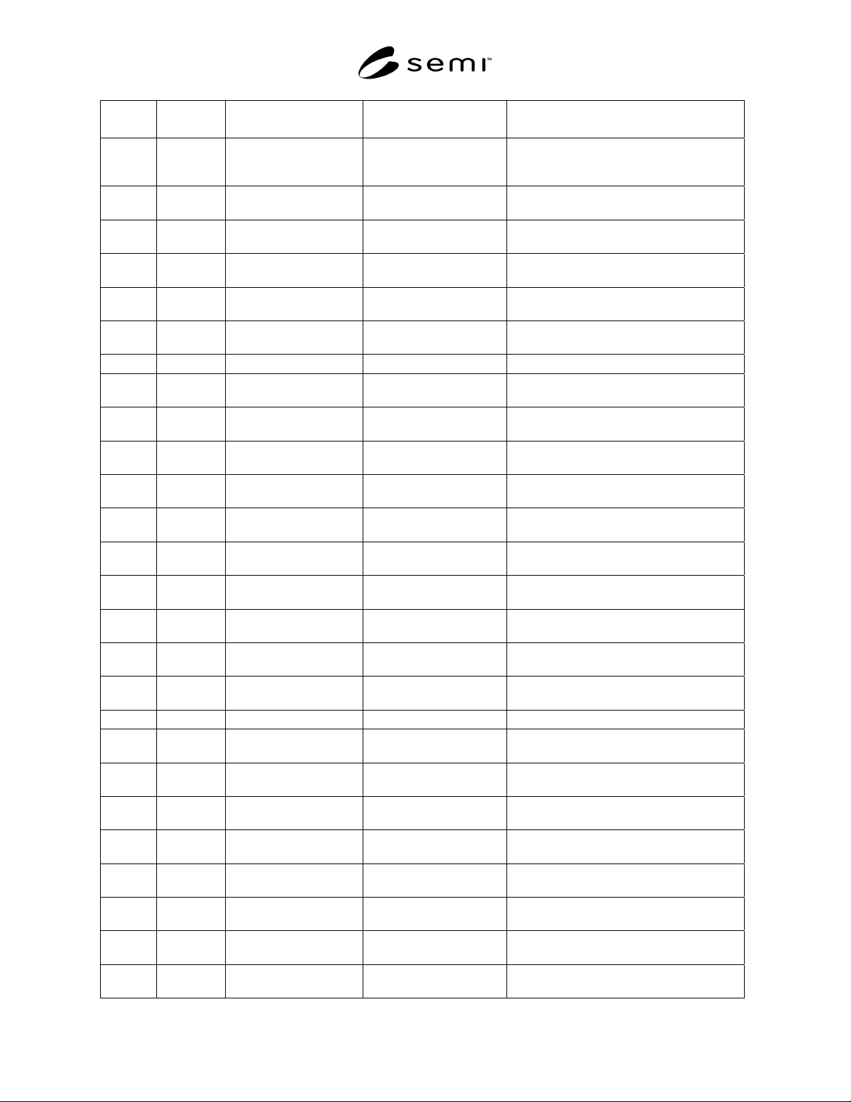
SEMI E1.9-0701 E2 © SEMI 1994, 2004 18 Symbol Used Figure Number Value Specified Datum Measured from Boundary or Feature Measured to z 28‡ 15 124.5 mm (4.90 in.) minimum horizontal datum plane top end of side c a ssette …
SEMI E1.9-0701
E2
© SEMI 1994, 2004 17
Symbol
Used
Figure
Number
Value Specified Datum Measured from Boundary or Feature Measured to
z2* 5, 8, 12 2 mm (0.08 in.)
maximum
horizontal datum plane bottom of carrier sensing pads and info pads
(when down) and advancing box sensing
pads (on FOUP only, see SEMI E47.1)
z3 8, 12 7 ± 1 mm
(0.28 ± 0.04 in.)
horizontal datum plane bottom of conveyor rail between x15 and
x16
z4 8, 12 15 ± 1 mm
(0.59 ± 0.04 in.)
horizontal datum plane cassette bottom outside of x16
z5 8, 9 10 mm (0.39 in.)
minimum)
horizontal datum plane top of pod latch-pin hole
z6† 6, 8, 9, 12 21 mm (0.83 in.)
maximum
horizontal datum plane top of cassette bottom domain
z7‡ 8, 12 35 ± 1 mm
(1.38 ± 0.04 in.)
horizontal datum plane bottom point of bottom side grip pits
z8† 6, 9, 12 33 mm (1.30 in.) horizontal datum plane bottom nominal wafer seating plane
z9‡ 8, 12 45 ± 1 mm
(1.77 ± 0.04 in.)
horizontal datum plane bottom of vertical sides of bottom side grip
pits
z10† 10, 11 0 ± 0.5 mm
(0.00 ± 0.02 in.)
each nominal wafer
seating plane
entire bottom of the wafer
z11† 10, 11 see Table 2 each nominal wafer
seating plane
encroachment of cassette side domains on
clearance above the wafer
z12† 6, 9, 10,
11, 12
see Table 2 each nominal wafer
seating plane
adjacent nominal wafer seating planes
z13‡ 7, 10 24 ± 1 mm
(0.94 ± 0.04 in.)
top nominal wafer
seating plane
bottom wall of top side grip pits
z14‡ 7, 10 1 ± 1 mm
(0.04 ± 0.04 in.)
top nominal wafer
seating plane
top point of top side grip pits
z15† 6, 9, 10 13 mm (0.51 in.)
minimum
top nominal wafer
seating plane
bottom of cassette top domain
z16‡ 7, 10 9 ± 1 mm
(0.35 ± 0.04 in.)
lowest point of underside
of top robotic flange
encroachment of cassette top domain on
space underneath robotic handling flange
z17‡ 7, 10 26 ± 1 mm
(1.02 ± 0.04 in.)
top nominal wafer
seating plane
bottom of top robotic handling flanges
z18 6, 7, 9, 10 30 mm (1.18 in.)
maximum
top nominal wafer
seating plane
top of cassette top domain
z19 8, 12 24 mm (0.94 in.) horizontal datum plane origin of radius of cassette sensing hole
z20‡ 8, 12 60 ± 1 mm
(2.36 ± 0.04 in.)
top nominal wafer
seating plane
top wall of bottom side grip pits
z21‡ 7, 10 9 ± 1 mm
(0.35 ± 0.04 in.)
top nominal wafer
seating plane
top of vertical sides of top side grip pits
z22 8, 12 20 mm (0.79 in.)
minimum
horizontal datum plane top of fork-lift pin hole and upper limit of
volume bounded by r10
z23† 10 3 mm (0.12 in.)
maximum
each nominal wafer
seating plane
bottom of wafer extraction volume
z24‡ 7, 10 4 ± 1 mm
(0.16 ± 0.04 in.)
lowest point of underside
of top robotic flange
top of top robotic handling flange
z25‡ None ± 1 mm (± 0.04 in.)
flatness over tag area
horizontal datum plane surface of top and bottom cassette
identification tag areas
z26* 5 9 mm (0.35 in.)
minimum
horizontal datum plane bottom of info pads (when up)
z27‡ 15 64.5 mm (2.54 in.)
maximum
horizontal datum plane bottom end of side cassette identification tag
area
SEMI E1.9-0701
E2
© SEMI 1994, 2004 18
Symbol
Used
Figure
Number
Value Specified Datum Measured from Boundary or Feature Measured to
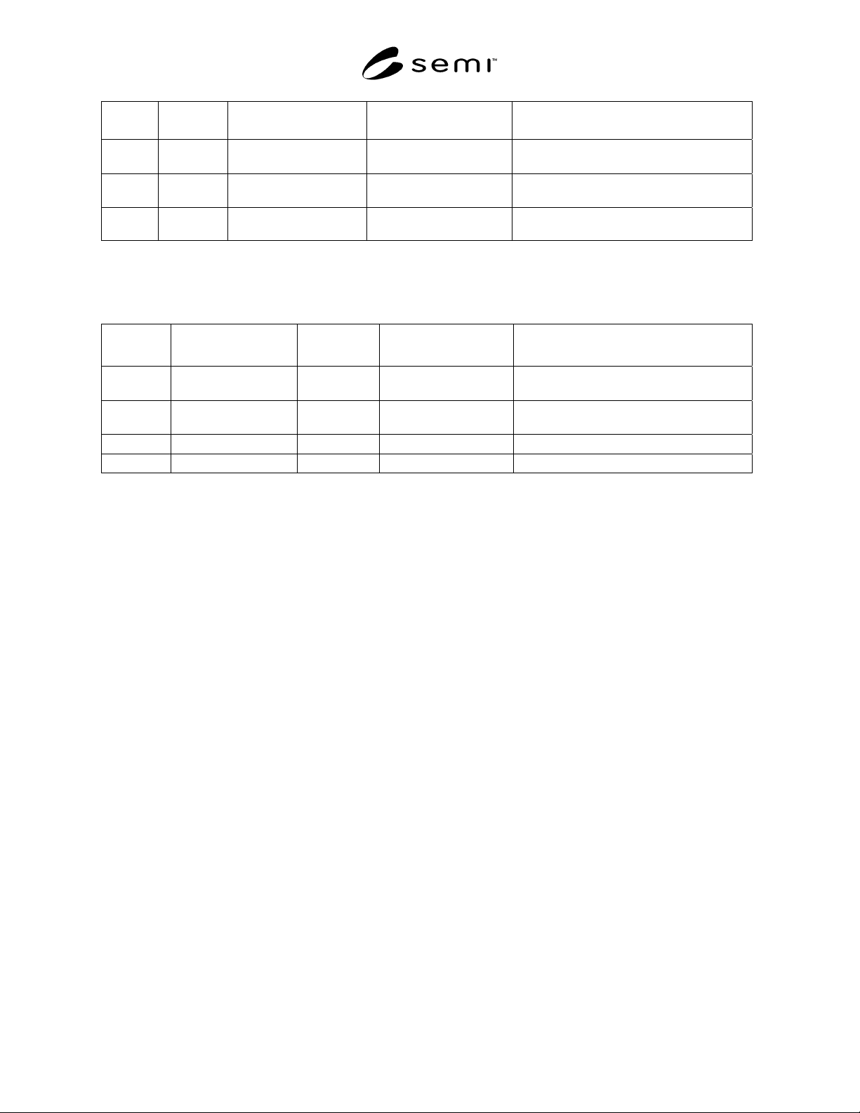
z28‡ 15 124.5 mm (4.90 in.)
minimum
horizontal datum plane top end of side cassette identification tag
area
z29 11 0.7 mm (0.028 in.)
maximum
each nominal wafer
seating plane
encroachment of cassette side domains
under wafer extraction volume
z99 15 94.5 mm (3.72 in.)
horizontal datum plane recommended center of label on side
cassette identification tag area
* These dimensions define external features that are also required for boxes.
† These dimensions define internal features that are also required for boxes with non-removable cassettes.
‡ These dimensions define optional features.
Table 2 Pitch and Capacity Options
Option
Number
Cassette Capacity
(c)
Wafer Pitch
(z12)
Wafer Clearance
(z11)
Resulting Cassette Height
(z8 – z1 + z12* (c – 1) + z18)
1 13 wafers 10 mm
(0.39 in.)
6 mm (0.24 in.)
minimum
183 mm (7.20 in.) maximum
2 25 wafers 10 mm
(0.39 in.)
6 mm (0.24 in.)
minimum
303 mm (11.93 in.) maximum
3 not yet defined
4 not yet defined
SEMI E1.9-0701
E2
© SEMI 1994, 2004 19
APPENDIX 1
APPLICATION NOTES
NOTE: The material in this appendix is an official part of
SEMI E1.9 and was approved by full letter ballot procedures
on December 18, 1998. The recommendations in this
appendix are optional and are not required to conform to this
standard.
A1-1 The cassette capacity is intended to include one
test wafer. It is recommended that process equipment
be designed for 12 or 24 product wafers, but tool
robotics should reach all slots.
NOTE: The carrier capacity need not be the same as the
transport group size, the process batch size, or the virtual
tracking unit size.
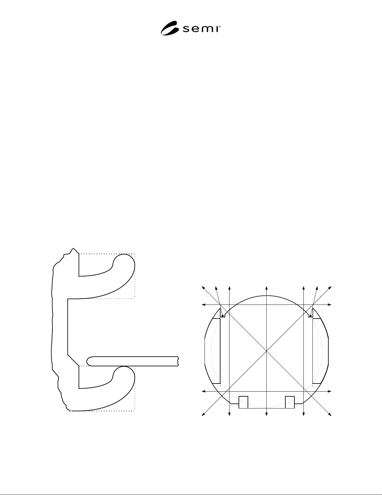
A1-2 The shape of the features holding the wafers is
not specified in this standard. However, a mizo tooth
shape (an exaggerated version of which is shown in
Figure A1-1) is recommended. It is also recommended
that the surface that touches the wafer have a large
radius to minimize stress on the wafer and the
supporting feature. It is recommended that the
supporting feature touch the wafer only on the back
side and far enough away from the edge to avoid
contact with the wafer notch (if any) in any radial
orientation.
wafer
tooth
Figure A1-1
Mizo Tooth
A1-3 In general, it is recommended that the wafer
notch and/or its fiducial identification marks be kept
toward the front of the cassette and the front of the
cassette top extend no farther than y14 from the facial
datum plane, so that the identification marks on the top
wafer can be read without removing the wafer.
A1-4 Extra clearance (larger than the pitch) has been
added below the bottom wafer (for non-random
sequential access to the wafers with a faster or less
precise robot) and above the top wafer (for accessing
the wafers in a vertical orientation), see Section 6.11.
A1-5 If wear at the kinematic couplings is a concern
with plastic cassettes, ceramic or metal inserts can be
used for the mating features.
A1-6 Skewness, warp, rock, and stiffness are implicitly
defined in the geometric tolerances.
A1-7 To increase the stability of the cassette on the
kinematic couplings, the points on the cassette bottom
that are the most distant from the lines connecting each
pair of coupling pins can be made as close as practical
to the horizontal datum plane so that the cassette cannot
tip very far off of the kinematic coupling pins.
A1-8 Figure A1-2 shows several paths for optically
sensing the presence and planarity of wafers in the
cassette. Also shown are the two vertical paths for
sensing how far the wafers protrude.
Figure A1-2
Optical Sensing Paths