semi合集-English.pdf - 第7229页
SEMI MF154-0305 © SEMI 2003, 2005 3 5 Terminology 5.1 Term s related to silicon technolog y, including the features and contaminants discussed in this guid e, are defined in SEMI M59. 6 Procedure 6.1 Procedures for exami…
SEMI MF154-0305 © SEMI 2003, 2005 2
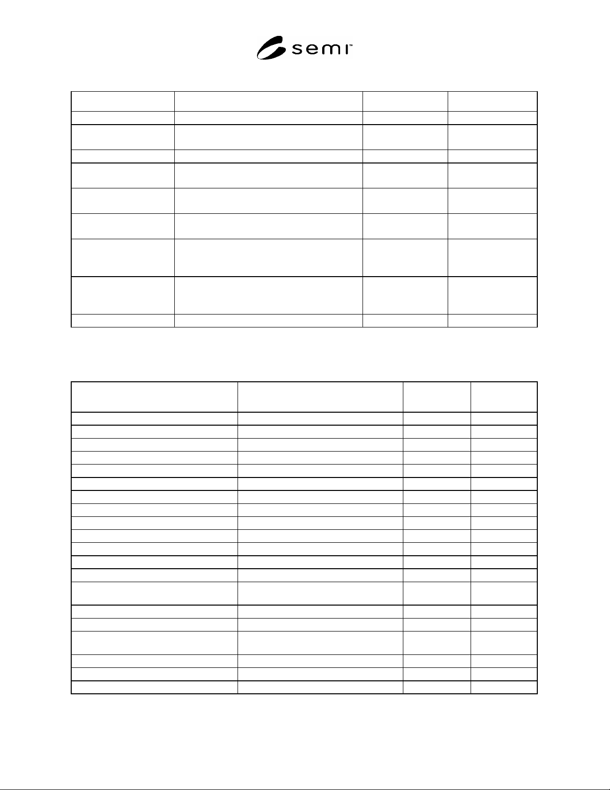
Table 1 Wafer Structural Defects
#1, #2, #3
Defect Common Synonyms and Acronyms Illustrating Figure(s) Relevant Standard(s)
Dislocation etch pit etch pit, pit 1-5 SEMI MF1725
Epitaxial stacking fault epi stacking fault, (ESF)
Epitaxial growth hillock
6-10 SEMI MF1726
Lineage Grain Boundary 11 SEMI MF1725
Oxidation induced stacking
fault
oxidation stacking fault, (OSF), oxidation induced
stacking fault (OISF)
12-18 SEMI MF1727
SEMI MF1809
Oxide precipitates bulk micro-defect, (BMD), bulk precipitate 19 SEMI MF1727
SEMI MF1809
Shallow pits S-pit, saucer pit 20-21 SEMI MF1727
SEMI MF1809
Slip slip lines 22-25 SEMI MF1725
SEMI MF1727
SEMI MF1809
Swirl 26-27 SEMI MF1725
SEMI MF1727
SEMI MF1809
Twin twin lamella, twin line 28-30 SEMI MF1725
#1
Magnifications given in the attached illustrations are for an original frame size of 50 mm × 50 mm, except as noted.
#2
Unless otherwise noted, all attached figures illustrate polished silicon wafer surfaces.
#3
Unless otherwise noted, all attached figures with magnified images were created using interference contrast microscope equipment.
Table 2 Polished Surface Visual Characteristics
Defect Common Synonyms and Acronyms
Illustrating
Figure(s)
Relevant
Standard
Area contamination Contamination, foreign matter, residue 31-32 SEMI MF523
Crack Cleavage, fracture 33-38 SEMI MF523
Crater Slurry ring 39 SEMI MF523
Crow's feet Contact damage 40 SEMI MF523
Dimple Depression 41-42 SEMI MF523
Dopant striation ring Striation 43 SEMI MF523
Edge chip Chip 44-47 SEMI MF523
Edge crack Crack 48 SEMI MF523
Edge crown 49 SEMI MF523
Epitaxial large point defect large light point defect, (LLPD), spike 50 SEMI MF523
Foreign matter Contamination, residue 51-52 SEMI MF523
Groove Polished over scratch, microscratch 53-54 SEMI MF523
Haze 55-56 SEMI MF523
Localized light scatterers (particle
contamination)
large light scatterers, (LLS) 57-58 SEMI MF523
Mound 59 SEMI MF523
Orange peel Roughness 60 SEMI MF523
Pits Air pocket, hole, crystal originated pit,
(COP) insufficient polish
61-63 SEMI MF523
Saw mark 64 SEMI MF523
Scratches Handling damage 65-67 SEMI MF523
Stain 68 SEMI MF523

SEMI MF154-0305 © SEMI 2003, 2005 3
5 Terminology
5.1 Terms related to silicon technology, including the features and contaminants discussed in this guide, are defined
in SEMI M59.
6 Procedure
6.1 Procedures for examining silicon wafers for the features and contaminants discussed in this guide are covered in
SEMI MF523, SEMI MF1725, SEMI MF1726, SEMI MF1727, SEMI MF1809, and SEMI MF1810.
7 Keywords
contaminant; defects; dislocation; epitaxial; fracture; preferential etch; scratch; shallow pit; silicon; slip; stacking
fault
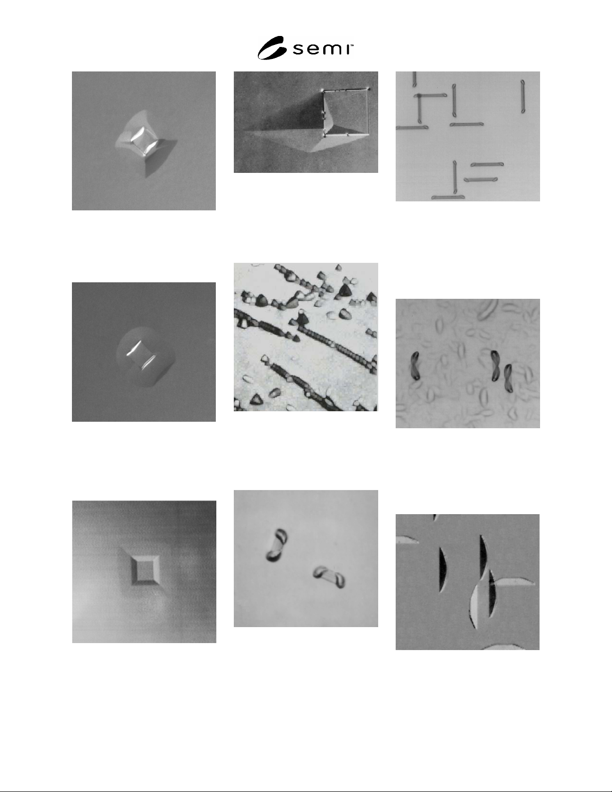
Figure 1
Dislocation Etch Pits on (111)
Silicon, Following 3-Min Sirtl
Etch, Magnification 110×
Figure 2
Dislocation Etch Pits on (110)
Silicon, Following 5-Min Wright
Etch, Magnification 110×
Figure 3
Dislocation Etch Pits on (100)
Silicon Following Schimmel (B)
Preferential Etch, Magnification
320×
Figure 4
Dislocation Etch Pits on (100)
Silicon Following Sirtl Etch,
Magnification 400×
Figure 5
Dislocation Etch Pits on (100)
Silicon Following 5-Min Wright
Etch, Magnification 200×
Figure 6
Epitaxial Stacking Faults on
(111) Following 4.2 m Dash etch,
Size Dependent Upon EPI
Thickness
SEMI MF154-0305 © SEMI 2003, 2005 4
Figure 7
Epitaxial Stacking Faults on
(100), No Preparation Required,
Size Dependent Upon EPI
Thickness
Figure 8
Epitaxial Stacking Faults on
(100), No Preparation Required,
Size Dependent Upon EPI
Thickness
Figure 9
Epitaxial Growth Hillock on
(100), No Preparation Required,
Size Dependent Upon EPI
Thickness
Figure 10
Epitaxial Stacking Faults on
(100), No Preparation Required,
Size Dependent Upon EPI
Thickness
Figure 11
Lineage on (111) Silicon
Following Preferential Etch,
Magnification 140×
Figure 12
Oxidation Induced Stacking
Faults on (100) Silicon Following
Oxidation and 4-min Wright
Etch, Magnification 200×
Figure 13
Oxidation Induced Stacking
Faults from Liquid Hone
Damage on a (100) Silicon
Polished Frontside Surface
Following Oxidation at 1100°C
and 1-min Schimmel Etch,
Magnification 1500×
Figure 14
Oxidation Induced Stacking
Faults from Liquid Hone
Damage on a (100) Etched Back
Surface Following Oxidation at
1100°C and 1-Min Schimmel
Etch, Magnification 1500×
Figure 15
Oxidation Induced Stacking
Faults on (100) Silicon Following
Oxidation and 3-Min Secco Etch,
Magnification 500×