semi合集-English.pdf - 第4192页
SEMI F72-1102 © SEMI 2002 3 11 Test Specimens 11.1 Specimens are to be sectioned to appropriate size for the particu lar AES instrum ent using a clean, dry hacksaw or dry low s p eed bandsaw. Any sample preparation shall…

SEMI F72-1102 © SEMI 2002 2
4.2 ASTM
1
Standards
ASTM E 673 — Standard Terminology Relating to
Surface Analysis
ASTM E 1078 — Standard Guide for Specimen
Handling in Auger Electron Spectroscopy and X-ray
Photoelectron Spectroscopy
ASTM E 1127 — Standard Guide for Depth Profiling
in Auger Electron Spectroscopy
NOTE 1: Unless otherwise indicated, all documents cited
shall be the latest published versions
5 Terminology
5.1 Terminology is per ASTM E 673 unless otherwise
specified.
5.2 Abbreviations and Acronyms
5.2.1 AES — Auger Electron Spectroscopy
5.3 Definitions
5.3.1 passivation — the chemical treatment of a
stainless steel surface with a mild oxidant for the
purpose of enhancing the corrosion resistant surface
film.
5.3.2 sampling volume — the volume in the sample
from which Auger electrons are detected. The electron
beam spot size or the scan area, and the acceptance
angle of the electron analyzer determine the lateral
dimensions. A length of three times the Auger electron
mean free path is considered the maximum depth
sensitivity. Sampling volume is dependent on the
sample material and TOA.
5.3.3 take-off angle (TOA) — the angle that the
collection lens forms with the sample plane.
6 Summary of Method
6.1 Data Acquisition
6.1.1 Acquire initial elemental survey and calculate
elemental composition of “as received” wetted surface.
6.1.2 Acquire a compositional depth profile by ion
etching to determine the relative abundance of C, O, Cr,
Fe and Ni. Additional elements may be included as
desired (i.e., molybdenum, silicon and nitrogen). The
thickness of the passive oxide layer and carbon is also
determined from the depth profile.
1 American Society for Testing and Materials, 100 Barr Harbor
Drive, West Conshohocken, Pennsylvania 19428-2959, USA.
Telephone: 610.832.9585, Fax: 610.832.9555 Website:
www.astm.org
6.2 Reporting — Data is provided consisting of:
6.2.1 An initial survey spectrum extending from
approximately 0 to 2000 eV.
6.2.2 A compositional depth profile plot including C,
O, Cr, Fe and Ni as a function of sputtering time.
6.2.3 A table of the as-received surface elemental
composition calculated from the initial survey
spectrum.
6.2.4 A table of the oxide thickness, the carbon
thickness, and the maximum of the Chromium to Iron
ratio calculated from the depth profile.
7 Possible Interferences
7.1 Cr and O — Carefully select windows for oxygen
and chromium to minimize interference. Monitor
individual windows after profile is complete to evaluate
effects. Some instruments may have enhanced ability
to compensate for overlaps.
8 Apparatus
8.1 Instrumentation — Any AES instrument equipped
with an ion gun may be used, whether it etches and
measures simultaneously or in alternating fashion. An
instrument that analyzes and etches in alternating
fashion should be evaluated to assure that no significant
oxygen level redeposits onto the sample surface
between etching intervals. The electron analyzer may
be of either the hemispherical or cylindrical mirror
analyzer (CMA) type. The electron energy analyzer
shall be of high enough energy resolution to permit
adequate separation of the Chromium KLL and Oxygen
KLL Auger peaks.
8.2 Instruments with geometries significantly different
from one another may provide analysis from different
sampling volumes. The incident electron beam energy,
the angle of the incident electron beam to the sample
plane, and the take-off angle must be recorded.
9 Reagents and Materials
9.1 Instrument Calibration Materials — Refer to
instrument manufacturer recommendations or ASTM E
1127 for standard materials.
10 Safety Precautions
10.1 This test method does not purport to address the
safety considerations associated with use of high
voltage, vacuum, and electron producing equipment.
The method assumes an AES analyst with adequate
skill level as well as knowledge of instrumentation and
associated safety precautions.
SEMI F72-1102 © SEMI 2002 3
11 Test Specimens
11.1 Specimens are to be sectioned to appropriate size
for the particular AES instrument using a clean, dry
hacksaw or dry low speed bandsaw. Any sample
preparation shall avoid introducing contamination onto
the surface to be measured. Clean noncontaminating
gloves and tweezers should be used to handle samples,
avoiding contact with the area of interest. In addition,
preparation must avoid excessive heating of the sample;
i.e., the surface temperature shall not exceed 50
o
C, to
avoid oxide growth or change in surface composition.
11.2 Sample preparation should preferably be done by
the component manufacturer. Following sectioning the
sample(s) are to be cleaned and packaged per the
manufacturer’s standard final cleaning and packaging
procedures.
11.3 If sample preparation is done by other than the
manufacturer, the sample(s) may be cleaned in DI water
and dried promptly. If the sample(s) are not to be
analyzed immediately they should be packaged by
wrapping in clean metal foil or sealing in cleanroom
quality nylon bags.
11.4 If sample preparation is done by other than the
manufacturer this shall be stated in the report narrative
and the analytical results are not to be interpreted as
indicative of the manufacturer’s quality of cleaning and
packaging procedures. A note to this effect shall be
included in all tables of reported results of the
composition of the surface.
11.5 After preparation, samples should be analyzed
promptly, with allowance for shipping times and
queuing time at the analyst.
12 Preparation of Apparatus
12.1 Instruments shall be routinely tested in
accordance with manufacturer recommendations to
assure proper performance. The instrument vacuum
shall be 1.0 × 10
-7
Torr or better during the analysis.
13 Calibration and Standardization
13.1 Instrument calibration for etch rates and
sensitivity factors shall be performed in accordance
with instrument manufacturer recommendations or
other established method.
14 Procedure
14.1 The sample is to be mounted in accordance with
manufacturer's recommendations and in a manner
consistent with ultra-high vacuum surface analytical
procedures. Some of these practices are detailed in
ASTM E 1078. The area to be analyzed should be
mounted parallel to the sample holder surface so that
the TOA is known.
14.2 Place the sample in the AES introduction chamber
for pumpdown. Transfer to the analytical chamber at
the manufacturer's recommended base pressure.
14.3 Align the sample with respect to the electron
beam and analyzer so that optimum count rate from the
desired analytical location is obtained. The surface area
to be analyzed should be free of sample preparation
debris, visible particles and large defect features, if
possible.
14.4 A large beam size or scan area should be used to
attempt measurement of a representative surface.
Elemental survey data (approximately 0-2000 eV) are
to be measured from the sample surface to determine
the elements present and their approximate surface
abundances. A signal-to-noise ratio of 2 is usually
adequate to ensure detection of elements present at one
atomic percent or greater levels. A typical survey
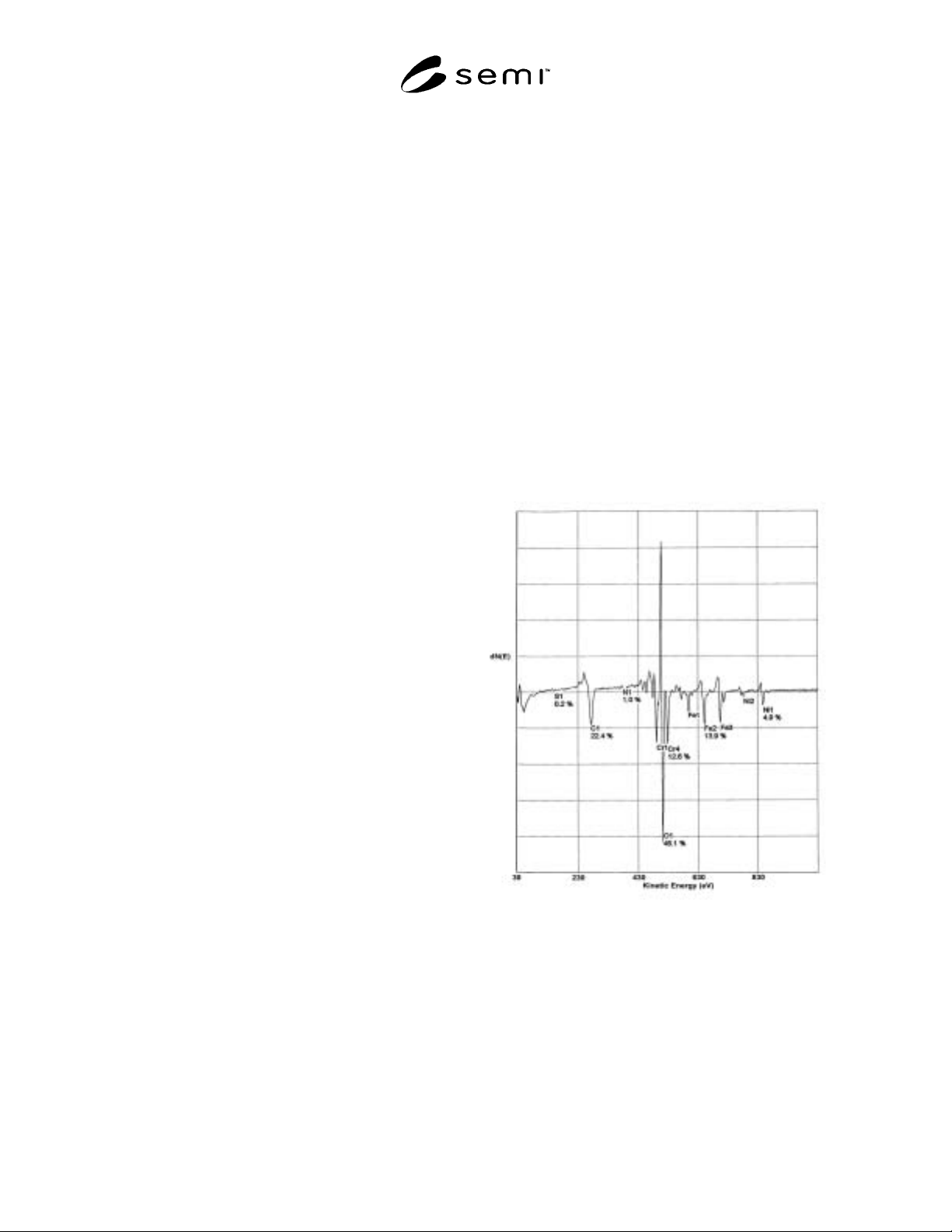
spectrum is shown in Figure 1.
Figure 1
Auger Spectrum of Stainless Steel Surface
14.5 Acquire a depth composition profile to determine
the relative abundances of Cr, Fe, Ni, O, and C. The
profile may be acquired in a simultaneous or an
alternating etch/data acquisition mode. Measurement
of each element shall be made at a frequency of at least
one data point every 5 Å within the first 50 Å and one
data point every 10 Å from 50 Å to the profile end. An
appropriate scan acquisition time is one that optimizes
SEMI F72-1102 © SEMI 2002 4
spectral resolution and signal/noise, and that has at least
ten data points in each spectral window. The depth
profile should be continued into the depth of the sample
until the Fe, Cr and Ni levels are approximately
constant.
14.6 Depth profile data are presented as signal intensity
of each element with etch time (i.e., depth), and as
atomic concentration with etch time. Depths may be
estimated from etch times by determination of the etch
rate on a known thickness of standard material. A
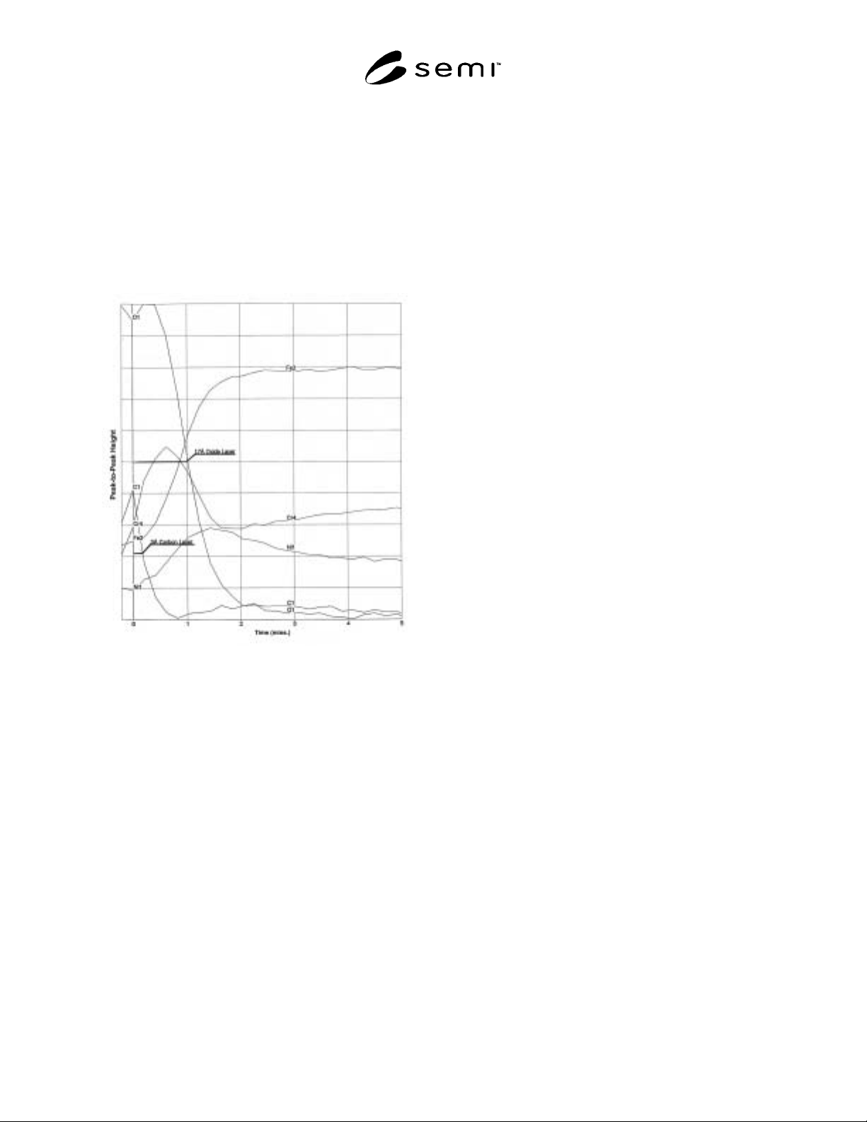
typical AES profile is shown in Figure 2.
Figure 2
Auger Depth Profile of Stainless Steel
15 Calculations and Interpretation of Results
15.1 Most manufacturers supply software for
calculation of the approximate elemental composition
from the survey spectrum and the depth profile data.
The elemental composition should be estimated using
sensitivity factors appropriate to the instrument, each
element, and resolution settings for each measurement.
AES spectra are considered only semiquantitative, due
to instrument geometry and the chemical form
dependency of each element's sensitivity factor.
Evaluations of elemental composition should therefore
be limited to similar samples analyzed on the same
instrument.
15.2 The signal intensity with etch time graph may be
used to calculate oxide thickness, defined as the point at
which the oxygen signal decreases to half its maximum
value. The thickness of surface carbon contamination
is calculated in the same way from the carbon signal.
15.3 Relative abundances of profiled elements are
recorded on the atomic concentration with etch time
graph.
16 Reporting Results
16.1 A tabular summary of estimated surface elemental
composition is to be supplied with its associated
elemental survey spectrum.
16.2 Tabular summaries of oxide thickness, thickness
of the region in which Cr concentration exceeds Fe
concentration, thickness of a surface Fe enrichment (if
present), and carbon thickness are to be supplied with
associated depth profile graphs.
16.3 Optionally, parameters such as maximum Cr/Fe
ratio may be reported. However, the value of the
maximum Cr/Fe ratio is subject to instrument geometry
and sensitivity factor variations, and should not be used
for primary evaluation purposes. Comparative
evaluations should only be made from data collected by
the same instrument with an identical protocol.
16.4 Data acquisition parameters, including instrument
geometry, electron beam size or scan area, and other
pertinent settings are to be supplied. The manufacturer
and model number of instrument used is to be reported.
Analyst identity and analysis date are also required
information. Each table and graph must be clearly
labeled with sample identification.
NOTICE: SEMI makes no warranties or
representations as to the suitability of the standards set
forth herein for any particular application. The
determination of the suitability of the standard is solely
the responsibility of the user. Users are cautioned to
refer to manufacturer's instructions, product labels,
product data sheets, and other relevant literature,
respecting any materials or equipment mentioned
herein. These standards are subject to change without
notice.
By publication of this standard, Semiconductor
Equipment and Materials International (SEMI) takes no
position respecting the validity of any patent rights or
copyrights asserted in connection with any items
mentioned in this standard. Users of this standard are
expressly advised that determination of any such patent
rights or copyrights, and the risk of infringement of
such rights are entirely their own responsibility.