semi合集-English.pdf - 第5276页
SEMI M46-1101 E © SEMI 2001 2 5.1.2 A rectify ing barrier, of kn own contact area, is form ed by placin g the sample in con tact with an electrolyte. 5.1.3 T he quality of the barrier is assessed usin g I- V and C-V m ea…

SEMI M46-1101
E
© SEMI 2001 1
SEMI M46-1101
E
TEST METHOD FOR MEASURING CARRIER CONCENTRATIONS IN
EPITAXIAL LAYER STRUCTURES BY ECV PROFILING
This test method was technically approved by the Global Compound Semiconductor Committee and is the
direct responsibility of the European Compound Semiconductor Materials Committee. Current edition
approved by the European Regional Standards Committee on June 29, 2001. Initially available at
www.semi.org December 2001; to be published March 2002.
E
This document was editorially modified in November 2001 to correct a typographical error. A change was
made to Section 7.3.3.
1 Purpose
1.1 The purpose of this document is to specify a
method to measure the carrier concentration and carrier
concentration vs. depth profile of epitaxial layers by
Electrochemical Capacitance Voltage ECV profiling.
2 Scope
2.1 This test method covers a procedure for measuring
the carrier concentration of epitaxial layers by ECV
profiling. This method focuses on improving the
accuracy and repeatability of the measurement by
standardizing the test conditions and reporting and by
routine calibration of the measurement.
2.2 This test method is intended to cover the majority
of routine samples measured. However, because of the
number of different materials encountered it cannot
cover every contingency.
2.3 This standard may involve hazardous materials.
This standard does not purport to address safety issues,
if any, associated with its use. It is the responsibility of
the users of this standard to establish appropriate safety
and health practices and determine the applicability of
regulatory limitations prior to use.
3 Referenced Standards
3.1 SEMI Standards
SEMI C1 — Specifications for Reagents
3.2 ASTM Standards
D1125-95 (1999) — Standard Test Methods for
Electrical Conductivity and Resistivity of Water
4 Terminology
4.1 bias — the potential applied to the sample with
respect to a reference electrode.
4.2 capacitance voltage CV measurements — electrical
measurements where the capacitance of a rectifying
barrier is measured as a function of applied bias and is a
measure of the net fixed ionized charge per unit
volume.
4.3 carrier concentration — the net fixed ionized
charge per unit volume. Equal to the free carrier
concentration if the dopant is fully ionized and the
material is free of traps.
4.4 current voltage IV measurements — electrical
measurements where the current through the rectifying
barrier is measured as a function of applied bias.
4.5 dissipation factor — the ratio of the real part to the
imaginary part of the complex admittance. It is a
measure of the non-ideality of the barrier.
4.6 electrochemical — chemical reaction in which
charge transfer takes place via an external circuit.
4.7 epitaxial layer — a layer of single crystal
semiconductor material grown on a host substrate
which determines its orientation.
4.8 excess area — the difference between the wetted
and illuminated areas.
4.9 flatband potential — the intercept on the voltage
axis of the 1/C
2
vs V plot. A measure of the built in
field or barrier height.
4.10 illuminated area — the area of the sample which
can be illuminated during electrochemical etching.
4.11 rectifying barrier — a potential gradient formed
at the junction between two materials which permits the
flow of charge in one direction only.
4.12 reference electrode — half cell which has a
constant electrode potential, such as a saturated calomel
electrode, SCE.
4.13 rest potential — the open circuit potential of the
sample with respect to the reference electrode.
4.14 wetted area — the area of contact between the
electrolyte and the sample.
5 Summary of Method
5.1 In this method, the carrier concentration of the
epitaxial layer is measured by the CV method.
5.1.1 Ohmic contacts are formed on the sample.

SEMI M46-1101
E
© SEMI 2001 2
5.1.2 A rectifying barrier, of known contact area, is
formed by placing the sample in contact with an
electrolyte.
5.1.3 The quality of the barrier is assessed using I-V
and C-V measurements.
5.1.4 From the measured C-V data the carrier
concentration of the layer is determined.
5.1.5 The sample is anodically etched to produce a new
barrier deeper in the material. The etch depth is
determined using Faraday’s law of electrolysis.
5.1.6 Sections 5.1.4 and 5.1.5 are repeated to generate
a carrier concentration vs. depth profile.
6 Interferences
6.1 Thin Layers — Diffusion of carriers into adjacent
regions set a fundamental resolution limit to the
measurement. In addition if the layer has a high sheet
resistivity this can also affect the value obtained.
6.2 Double Layer Capacitance — A limitation
imposed by the physical nature of the
electrolyte/semiconductor barrier which sets an upper
limit to the measured carrier concentration, for accurate
measurements, of 1 × 10
19
cm
-3
. The technique can be
used beyond this value, but with progressive
degradation.
6.3 Etch Well Uniformity
6.3.1 Etch Well Flatness — Non-uniformity increases
the effective area and may result in the measurement
not being wholly made in the layer of interest. The
main causes of non-uniformity are gas bubbles,
inadequate electrolyte circulation and uneven
illumination.
6.3.2 Etch Well Roughness — indicates poor etching
and has a deleterious effect on the measurements.
Generally overcome by selecting a more appropriate
electrolyte and/or etching conditions.
6.4 Non-Ideal Electrical Characteristics
6.4.1 Series Resistance — From the contacts, sample
and electrolyte affect the accuracy of the measurements.
This effect is minimized by using a highly conductive
electrolyte, making large area ohmic contacts and by
employing a low measurement frequency.
6.4.2 Leakage Currents — Parallel conduction can
affect the accuracy of the measurement. Its influence is
reduced by employing a high measurement frequency.
6.4.3 Large Excess Area — Can give rise to errors on
n-type material particularly when profiling Hi-Lo
structures. The excess area is electrolyte dependent but
is mainly affected by the quality of the seal used to
define the area. Large excess areas indicate a poor seal
and are corrected by replacing the seal.
6.5 Hi-Lo Structures — Measurement is subject to
inaccuracy due to carrier diffusion and excess area
errors. For accurate measurements, chemically etch to
the layer of interest before measurement.
6.6 Contact Quality — Non-Ohmic or high resistance
contacts have a deleterious effect on the measurement.
Contacts should be checked by measuring the resistance
between two similar contacts and then reversing the
current direction and repeating the measurement.
6.7 Surface and Deep States — Cause the measured
capacitance to be frequency dependent and/or
dependent on the rate at which the bias is changed.
Usually resolved by using a high measurement
frequency. This should not be confused with the
frequency dependence which is more usually attributed
to high series resistance.
6.8 Surface Films — Have a deleterious effect on the
capacitance measurement. Film formation should be
avoided by using an appropriate electrolyte, control of
the etching bias and time and by electrolyte circulation.
6.9 Surface Roughness — The surface of the sample
should be smooth and free of features that would affect
the action of the seal.
6.10 Light — Light can affect the capacitance
measurement, so the sample must be placed in a dark
environment during the measurement.
6.11 Sample Loading — The accuracy of the
measurement depends on the repeatability of the area. If
a compliant seal is involved, such as a plastic ring, the
sample should be held in contact with the seal by
applying a controlled and constant force. No relative
lateral movement should take place during the loading
process.
6.12 Ring Variability — The condition of the ring has a
large effect on the measurement. Good seals will have a
small to zero excess area and exhibit a well defined and
reproducible contact area.
7 Apparatus
7.1 Measurement of Etch Well and Ring Areas —
Measuring microscope with either an XY stage, with a
linear resolution of 0.01 mm or better, or a camera and
image processing system capable of measuring an area
of 0.1 cm
2
to better than 0.5%.
7.2 Measurement of Etch Well Flatness — (Optional)
A means such as a stylus profiler for checking the
flatness and roughness of the etch well. In most cases
visual inspection of the etch well, for a mirror like
appearance, is sufficient indication of low roughness.
SEMI M46-1101
E
© SEMI 2001 3
7.3 Instrumentation
7.3.1 Capacitance Meter — Capable of measuring
values up to 300 nF, employing a test signal of
amplitude less than 100 mV RMS. The measurement
frequency should be typically between 1 and 100 kHz.
7.3.2 Equivalent Circuit Model — The meter should
assume a parallel circuit model for the
electrolyte/semiconductor interface and provision
should be made to compensate for the large series
resistance of the electrolyte and contacts.
7.3.3 Potentiostat — Capable of maintaining the
potential of the sample with respect to a reference
electrode constant to ±5mV during the measurement
and with a reference input impedance of > 10
13
Ohms.
7.3.4 Light Source — A source of uniform illumination
of above band gap energy for etching n-type materials.
7.4 Sample Holder
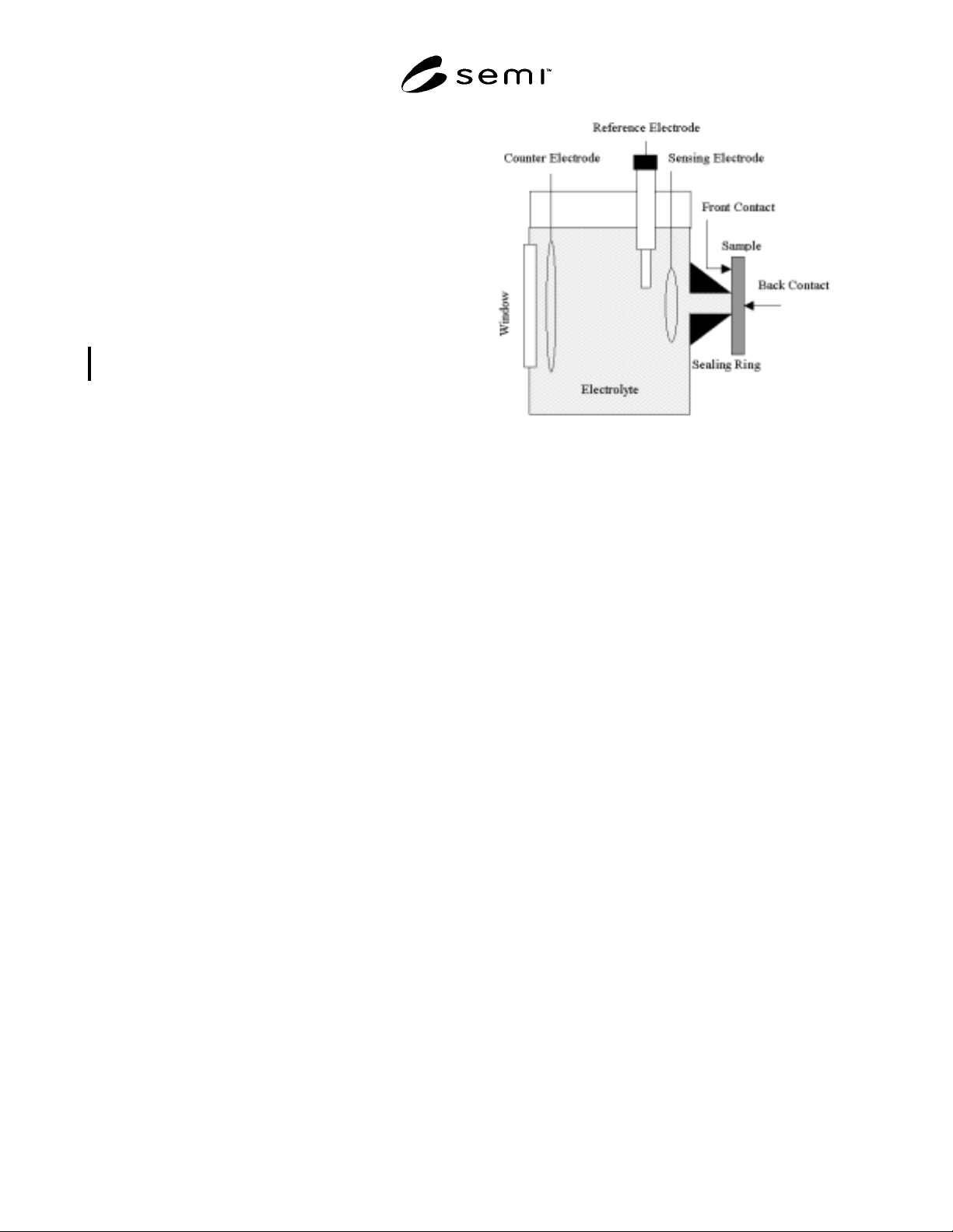
7.4.1 Electrochemical Cell — Used to hold the sample,
contain the electrolyte and support the sealing ring and
other electrodes, see Figure 1.
7.4.1.1 Sealing Ring — A corrosion resistant ring
which forms a seal between the electrolyte and the
sample. This ring defines the measurement area which
should be reproducible and well defined. The ring area
should not be less than 0.008 cm
2
and the
reproducibility between runs should be better than ±
3%. Large ring areas (typically ≥ 0.1 cm
2
) are preferred
for more accurate measurements.
7.4.1.2 Reference Electrode — Used to control the
sample bias via a potentiostat.
7.4.1.3 Counter Electrode — The bias and test signals
are applied between this electrode and the sample.
Figure 1
Electrochemical Cell
7.4.1.4 Sensing Electrode — Placed close to the
sample-electrolyte interface and used to measure the
admittance of the sample.
7.4.1.5 Sample Contacts — Ohmic contacts to the front
and/or back surface of the sample for the purpose of
applying bias.
8 Reagents and Materials
8.1 Purity of Reagents — All chemicals for which such
specifications exist shall conform to SEMI C1.
8.2 Purity of Water — Use either distilled or de-
ionized water having a resistivity greater than
2 MOhm•cm at 25
o
C as determined by the Non-Referee
Test of Test Methods D 1125.
8.3 Selection of Electrolyte — The choice of
electrolyte is not defined by this standard and is up to
the discretion of the user or by agreement between the
customer and the supplier.
8.3.1 InP, GaAs and Related Compounds — Preferred
electrolyte, Na
2
.EDTA (0.1 M) basified with
ethylenediamine to a pH of 10, although other
electrolytes can be satisfactorily used.
NOTE 1: Preferred electrolyte, see reference
“Electrochemical C-V Profiling of Heterojunction Device
Structures” A.C.Seabaugh et al. IEEE Trans on Electron Dev
36 No 2 (1989) 309-313.
9 Safety Precautions
9.1 The electrolytes used are potentially hazardous.
Read the Materials Safety Data Sheets before
attempting to prepare the electrolytes. Use safety