semi合集-English.pdf - 第7522页
SEMI MF1727-0304 © SEMI 2003, 2004 3 9 Sampling 9.1 Select specimens to represent the lot to be tested as specified in producer/consumer a g reements. 10 Specimen Preparation 10.1 Commonly this practi ce may be used for …

SEMI MF1727-0304 © SEMI 2003, 2004 2
3.7 Wafers, particularly <111> orientation, may show
lower shallow-pit defect density when the back surface
of the wafer is gettered. Backside gettering should be
noted in the sample classification when data are
reported.
4 Referenced Standards
4.1 SEMI Standards
SEMI C3.19 — Standard for Hydrogen (H
2
) 99.9995%
Quality
SEMI C28 — Specifications and Guidelines for
Hydrofluoric Acid
SEMI C54 — Specifications and Guidelines for
Oxygen
SEMI MF1241 — Terminology of Silicon Technology
SEMI MF1809 — Guide for Selection and Use of
Etching Solutions to Delineate Structural Defects in
Silicon
SEMI MF1810 — Test Method for Counting
Preferentially Etched or Decorated Surface Defects in
Silicon Wafers
4.2 ASTM Standard
1
D 5127 — Guide for Ultra Pure Water Used in the
Electronics and Semiconductor Industry
NOTICE: Unless otherwise indicated, all documents
cited shall be the latest published versions.
5 Terminology
5.1 Defect-related terminology may be found in SEMI
MF1241.
6 Summary of Practice
6.1 Wet oxidation is used to generate or highlight
defects, or both, in silicon wafers. This oxidation may
also simulate simple device production processes.
6.2 The defects are revealed subsequently by
preferential etching and examination by interference
contrast microscopy according to referenced SEMI
standards.
7 Apparatus
7.1 Oxidation Furnace — furnace shall be consistent
with the intended process application and shall sustain a
designated temperature with uniformity less than ± 5° C
over a zone at least 0.3-m long.
1 Annual Book of ASTM Standards, Vol 11.01. ASTM International,
100 Barr Harbor Drive, West Conshohocken, PA 19428. Telephone:
610-832-9500. Fax: 610-832-9555. Website:
www.astm.org
.
7.2 Steam Source — Wet oxidation shall be carried out
using a pyrogenic steam generator to provide steam.
7.3 Working Chamber — A pure, fused quartz, silicon
carbide, or silicon tube of an inside diameter sufficient
to hold the specimen wafers. The inlet end shall be
fitted with the appropriate pyrogenic torch apparatus.
The exhaust end shall be fitted to exhaust the process
gases to satisfy applicable environmental requirements
and prevent back streaming of outside air into the
working chamber.
7.4 Wafer Boat — A quartz, silicon or silicon carbide
fixture for holding the specimen wafers either parallel
or perpendicular to the gas flow in the furnace.
7.5 Pickup Tool — A manual or automated transfer
tool fitted with a nonmetallic material such as quartz or
TFE-fluorocarbon. The pickup tool shall be
constructed so that no metal can contact the specimen
wafer.
8 Reagents and Materials
8.1 Purity of Reagents — Chemicals shall conform to
the assay and impurity levels of Grade 1 SEMI
Specifications where they exist. Reagents for which
SEMI specifications have not been developed shall
conform to the specifications of the Committee on
Analytical Reagents of the American Chemical
Society,
2
where such specifications are available.
Gases shall conform to the purity requirements of the
cited SEMI specifications. Other grades may be used
provided it is first ascertained that the reagent is of
sufficiently high purity to permit its use without
lessening the accuracy of the determination.
8.2 Purity of Water — Reference to water shall be
understood to mean Type E-3 or better water as
described in ASTM Guide D 5127.
8.3 Hydrofluoric Acid — Concentrated, in accordance
with Grade 1 of SEMI C28.
8.4 Hydrogen Gas — In accordance with SEMI C3.19,
for use in pyrogenic steam generator.
8.5 Oxygen Gas — In accordance with SEMI C54, for
use both as furnace ambient and in pyrogenic steam
generator.
2 Reagent Chemicals, American Chemical Society Specifications,
American Chemical Society, Washington, DC. For suggestions on the
testing of reagents not listed by the American Chemical Society, see
Analar Standards for Laboratory Chemicals, BDH Ltd., Poole,
Dorset, U.K., and the United States Pharmacopeia and National
Formulary, U.S. Pharmacopeial Convention, Inc., (USPC), Rockville,
MD.
SEMI MF1727-0304 © SEMI 2003, 2004 3
9 Sampling
9.1 Select specimens to represent the lot to be tested as
specified in producer/consumer agreements.
10 Specimen Preparation
10.1 Commonly this practice may be used for wafers
as they are received; however, the parties using this
practice may establish a uniform cleaning procedure
before oxidation.
11 Preparation of Apparatus
11.1 The oxidation furnace tube (working chamber)
and associated quartzware shall be maintained in a state
suitable for producing oxides appropriate for the
process for which the wafers are being tested.
11.2 Immediately before use, clean the pickup tool
using standard industry practices.
12 Procedure
12.1 Handle wafers only with a clean, nonmetallic
pickup tool or automated transfer unit to avoid
scratching or contaminating the surface.
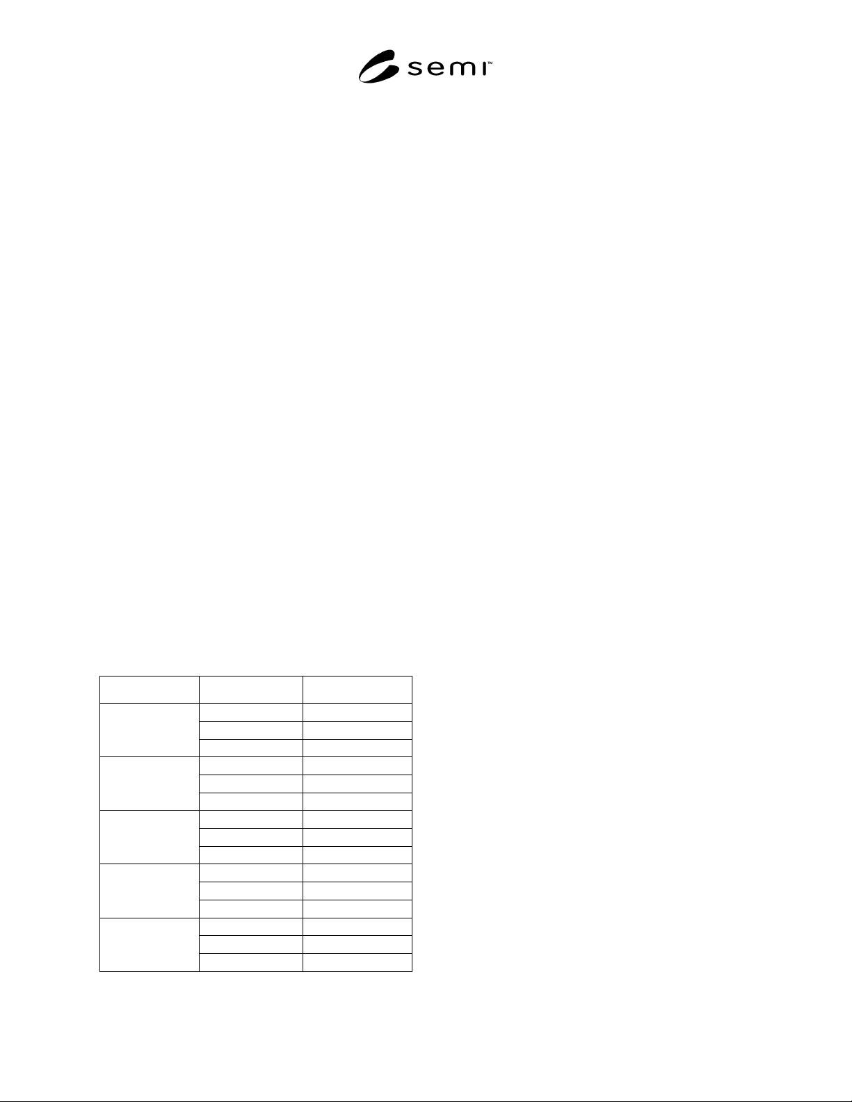
12.2 Oxidize the wafers by the thermal sequence listed
in Table 1 or by a process acceptable to both producer
and consumer.
12.2.1 Caution — Pyrogenic steam oxidation uses
heated hydrogen and oxygen to grow a wet oxide layer.
Improper or uncontrolled combination of these gases
can result in fire or explosion.
12.2.2 Preheat the furnace to the push temperature.
Table 1 Oxidation Procedure
Step Function Conditions
Ambient Dry Oxygen
Temperature 800° C
1. Push (Load)
Push Rate 200 mm/minute
Ambient Dry Oxygen
Ramp Rate + 5° C/minute
2. Temperature
Ramp
Final Temperature 1100° C
Ambient Steam (wet oxide)
Temperature 1100° C
3. Oxidation
Time 60 minute
Ambient Dry Oxygen
Ramp Rate –3° C/minute
4. Temperature
Ramp
Final Temperature 800° C
Ambient Dry Oxygen
Temperature 800° C
5. Pull (Unload)
Pull Rate 200 mm/minute
12.2.3 Load the specimen wafers into the wafer boat,
being careful to avoid binding, scratching, or
contamination.
12.2.4 Insert the boat into the hot zone at the rate called
for in the thermal sequence being employed. The wafer
boat shall be centered in the uniform hot zone.
12.2.5 Follow the ramp up, oxidation, ramp down, and
pull procedures as specified in the thermal sequence
being employed.
12.2.6 Because silicon wafers and quartz accessories
are extremely hot when they are removed from the
oxidation furnace, allow the materials adequate time to
cool before handling.
12.3 Transfer the room temperature wafers from the
quartz boat to a wafer carrier using the pickup tool or
automated transfer unit.
12.4 Remove the thermal oxide layer using
hydrofluoric acid for 2 min followed by water rinse and
spin dry.
12.4.1 Caution — Hydrofluoric acid solutions are
particularly hazardous and specific preventive measures
must be strictly observed. Safety or protective gear
should be worn while handling acid solutions. Safety
requirements vary, but the essential items are: plastic
gloves, safety glasses, face shield, acid gown, and shoe
covers.
12.5 Select and use an appropriate etching solution as
described in SEMI MF1809 to allow defect delineation
while removing 4 µm (or another amount as agreed
upon between the parties to the test) of silicon from the
surface being evaluated.
12.6 Count and report the density of observed defects
using SEMI MF1810.
13 Keywords
13.1 defects; dislocation; epitaxy; hillock;
imperfections; oxidation; preferential etch; shallow pit;
silicon; slip; stacking fault; swirl

SEMI MF1727-0304 © SEMI 2003, 2004 4
NOTICE: SEMI makes no warranties or
representations as to the suitability of the standards set
forth herein for any particular application. The
determination of the suitability of the standard is solely
the responsibility of the user. Users are cautioned to
refer to manufacturer' s instructions, product labels,
product data sheets, and other relevant literature,
respecting any materials or equipment mentioned
herein. These standards are subject to change without
notice.
By publication of this standard, Semiconductor
Equipment and Materials International (SEMI) takes no
position respecting the validity of any patent rights or
copyrights asserted in connection with any items
mentioned in this standard. Users of this standard are
expressly advised that determination of any such patent
rights or copyrights, and the risk of infringement of
such rights are entirely their own responsibility.
Copyright by SEMI® (Semiconductor Equipment and Materials
International), 3081 Zanker Road, San Jose, CA 95134. Reproduction o
f
the contents in whole or in part is forbidden without express written
consent of SEMI.