semi合集-English.pdf - 第4542页
SEMI D26-1000 © SEM I 2000 1 SEMI D26-1000 PROVISIONA L SPECIFICATION FOR LA RGE AREA M A SKS FOR FL AT PANEL DISPLAYS (NORTH A MERICA) This specif ication was technic ally approved by the Global Flat Panel Displa y Comm…
SEMI D25-0600
E
© SEMI 2000, 2003 24
APPENDIX 3
NOTE: The material in this appendix is an official part of SEMI D25 and was approved by full letter ballot procedures on April
21, 2000 by the Japanese Regional Standards Committee.
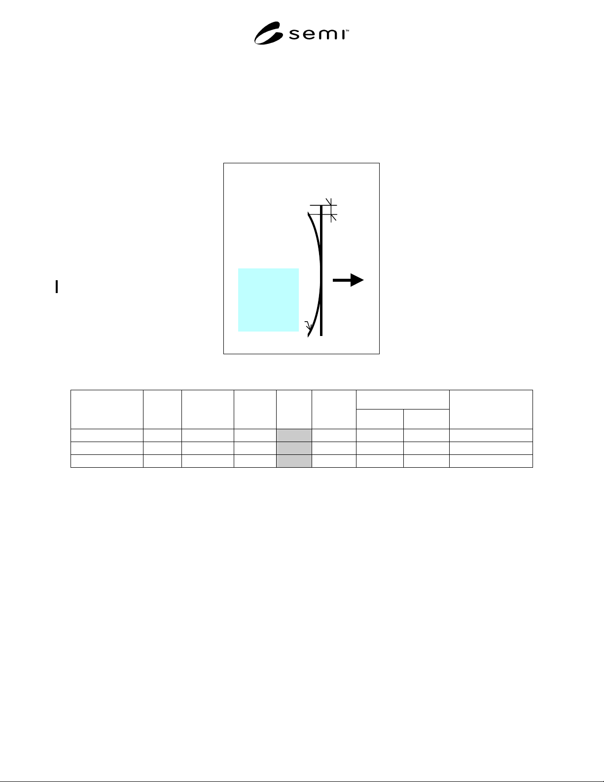
A3-1 Sag Caused by Acceleration
Glass Loading Method
During Transport
Example
Sag resulting
from 1G
added force
1G
Shrinkage
Unit = mm
Substrate Dimensions
Substrate Size G Value Support
Method
Span Sag Curved
Shrinkage
Long Edge Short Edge
Memo
800 × 950 × 0.7
1 4 --
20 1.4 950 800
Sag is for substrates
2 800 52 9.0 950 800 supported in
950 103 30.2 950 800 horizontal.
NOTE: Calculated by Asahi Glass Company
NOTICE: SEMI makes no warranties or representations as to the suitability of the standard set forth herein for any
particular application. The determination of the suitability of the standard is solely the responsibility of the user.
Users are cautioned to refer to manufacturer’s instructions, product labels, product data sheets, and other relevant
literature respecting any materials mentioned herein. These standards are subject to change without notice.
The user’s attention is called to the possibility that compliance with this standard may require use of copyrighted
material or of an invention covered by patent rights. By publication of this standard, SEMI takes no position
respecting the validity of any patent rights or copyrights asserted in connection with any item mentioned in this
standard. Users of this standard are expressly advised that determination of any such patent rights or copyrights, and
the risk of infringement of such rights, are entirely their own responsibility.
Copyright by SEMI® (Semiconductor Equipment and Materials
International), 3081 Zanker Road, San Jose, CA 95134. Reproduction o
f
the contents in whole or in part is forbidden without express written
consent of SEMI.

SEMI D26-1000 © SEMI 20001
SEMI D26-1000
PROVISIONAL SPECIFICATION FOR LARGE AREA MASKS FOR FLAT
PANEL DISPLAYS (NORTH AMERICA)
This specification was technically approved by the Global Flat Panel Display Committee and is the direct
responsibility of the North American Flat Panel Display Committee. Current edition approved by the North
American Regional Standards Committee on July 14, 2000. Initially available on SEMI OnLine August
2000; to be published October 2000.
1 Purpose
1.1 This specification establishes a set of standards to
assist in specifying and ordering large area masks for
the Flat Panel Display industry. A major objective is to
improve the cycle time, order process efficiency and
reduce the overall cost of manufacturing for both the
mask maker and the customer.
1.2 This specification is intended for use in North
America as an emerging market. However, the
applicability of this specification is not restricted or
limited to this region alone. This standard was
developed to address a North American need for a
common set of requirements for specifying,
manufacturing, and ordering large area masks.
2 Scope
2.1 The following areas are covered by this document:
2.1.1 Registration and Accuracy
2.1.2 Critical Dimensions
2.1.3 Centrality
2.1.4 Pellicles
2.1.5 Edge Length and Thickness
2.1.6 Symbology
2.1.7 Data Formats
2.1.8 Auto Inspection Artifacts
2.1.9 Product Labeling
2.2 This specification is being issued so that the
industry may evaluate the concept covered before its
adoption as a full standard. It is expected that initial
application will occur mostly in North America,
however, nothing in this standard limits its use to this
market region.
2.3 This standard does not purport to address safety
issues, if any, associated with its use. It is the
responsibility of the user of these standards to establish
appropriate safety and health practices and determine
the applicability of regulatory limitations prior to use.
3 Limitations
3.1 The document does not seek to be comprehensive.
Instead, the areas listed are meant to help move the
current industry towards an agreed upon set of
standards that are useful in reducing the overall cost of
supplying masks for use by FPD manufacturers. The
document only describes 1X full field masks up to 620
× 720 mm for all display types except for Plasma, TN
and STN LCD technologies.
4 Referenced Standards
NOTE: As listed or revised, all documents cited shall be the
latest publications of adopted standards.
4.1 SEMI Standards
SEMI D6 — Specification for Edge Length and
Thickness for Flat Panel Display Mask Substrates
SEMI P1 — Specification for Hard Surface Photomask
Substrates
SEMI P5 — Specification for Pellicles
SEMI P6 — Specification for Registration Marks for
Photomasks
SEMI T8 — Specification for Marking of Glass Flat
Panel Display Substrates with a Two-Dimensional
Matrix Code Symbol
4.2 AIM International Technical Specifications
1
AIM International Symbology Specification – Data
Matrix
5 Terminology
Each section of the document defines the terms used in
that section, with the exception of:
5.1 alignment bar, of a data matrix symbol — A solid
line of contiguous filled cells abutting a line of
alternatively filled and empty cells (AIM International
Symbology Specification Data Matrix)
1 AIM International Inc., 11860 Sunrise Valley Drive, Suite 100,
Reston, VA 20191, tel y703.391.7621, fax 703.391.7624

SEMI D26-1000 © SEMI 2000 2
5.2 border column — The outermost column of a data
matrix code symbol. This column is a portion of the
finder pattern.
5.3 border row — The outermost row of a data matrix
code symbol. This row is a portion of the finder pattern.
5.4 cell, of a data matrix code symbol — The area
within which a dot may be placed to indicate a binary
value.
6 Ordering Information
6.1 Purchase orders for substrates furnished to this
specification shall include the following items:
Checklist:
6.2 Edge length
6.3 Long reference edge
6.4 Short reference edge
6.5 Orientation corner dimensions
6.6 Quality edge area exclusion
6.7 Thickness
6.8 Tolerance for all specified dimensions
6.9 Warp
6.10 Marking
6.10.1 Marking message characters
6.10.1.1 Quantity (46 to mm, where mm = 72)
6.10.1.2 Content of message characters related to
Customer Specification Number, and message
characters 47 and up, if present.
6.10.1.3 Location of mark, if different from Section
9.5.5
7 Requirements
7.1 Materials Specification — Substrate material shall
be specified as high thermal expansion (HTE), medium
thermal expansion (MTE), low thermal expansion
(LTE), or ultra low thermal expansion (ULTE).
Examples of HTE materials are soda lime glasses;
examples of ULTE materials are synthetic quartz
glasses. Substrate materials shall conform to thermal
expansion and optical transmittance characteristics
specified in SEMI P1. Selected physical properties of
HTE, MTE, LTE, and ULTE materials are provided for
information in SEMI P1.
7.2 Overlay — Overlay refers to alignment of the
printed pattern of one mask to another of the same set.
Overlay error shall not exceed ± 6.0 µm for soda lime
plates and ± 2.0 µm for quartz plates when plate
temperature is maintained within ± 1°C. Alignment or
registration marks per SEMI P6 may be used to
facilitate measurements.
7.3 Positional Accuracy — Relation between actual
and desired locations of a printed feature on a glass
substrate. This is a tolerance to be agreed upon by the
end user and mask designer. The following guidelines
should be used, with measurements being taken in a
temperature and humidity controlled environment:
• ± 0.0157 µm/mm/ °C for soda lime masks
• ± 0.00394 µm/mm/ °C for quartz masks
Dimensioning from a central reference point shall be
used.
7.4 Critical Dimensions (CD) — The gauging or
measurement process is fundamental to manufacturing
of masks. The purpose of this section is to define
standard CD patterns to provide consistent evaluation
and testing of micropatterning equipment, metrology
instruments and processes used in large area mask
photomask manufacturing.
7.4.1 Figures 1 and 2 are intended to illustrate the
proper layout of each pattern cell and to define
appropriate design elements used within each basic cell.
The user will determine all appropriate dimensions for
the feature as they apply to specific processing/
equipment situations.
7.4.2 L-bar cell (see Figure 1) — The L-bar cell is
designed to be a measurement site for isolated features
as well as line and space groups in orthogonal axes. The
basic cell consists of one or more groups of nested L-
shaped lines at a specific pitch. The pitch is defined as
twice the nominal feature width. The center L-bar of
each group shall extend beyond the ends of the other L-
bars by at least 10µm. This implies that the number of
bars is odd.
7.4.3 Contact array cell (see Figure 2) — The contact
array cell is designed to provide resolution and proxim-
ity effect information over a wide range of contact
sizes. The design elements will consist of a 5 × 5 con-
tact array and an isolated contact. The 5 × 5 array will
produce the maximal proximity for the center contact.
7.4.4 A label to indicate the nominal feature width
must be placed near each basic cell. The labels must be
of a clearly printable size. The details of the pattern
cells, such as the orientation, magnitude, range of line
widths and polarity of tone (clearfield vs. darkfield)
shall be defined by the user.
7.4.4.1 The target CD should closely represent the size
of the most critical feature in the end user’s process, not
necessarily the minimum feature. A reasonable
tolerance is ± 10% of the target CD.