semi合集-English.pdf - 第7304页
SEMI MF1152-0305 © SEMI 2003, 2005 3 9.3 Incl ude horizontal and vertic al axes and label the lines on t h e notch form and depth templat e as shown in Fi gure 1. NOTE: In use the template is rotated 90° counterclo ckwis…

SEMI MF1152-0305 © SEMI 2003, 2005 2
NOTICE: Unless otherwise indicated, all documents cited shall be the latest published versions.
5 Summary of Test Method
5.1 The wafer is aligned in position on an optical comparator and the image of the notch is compared with a series
of templates projected on the screen of the comparator.
5.2 First, the wafer is aligned so that the sides of the image of the notch contact the image of the alignment pin for
fixing the position of the wafer in use. In this case, the image of the notch bottom must lie on or below the
designated line on the notch form/depth template and the image of the wafer edge must lie on or above another
designated line on the template.
5.3 The wafer is then aligned so that the image of the wafer edge coincides with the wafer periphery line on the
template. In this case, the image of the notch bottom must lie between maximum and minimum lines on the
template.
5.4 The image of the notch sides are compared with a series of angles on the notch angle template and the angle that
makes the best fit is chosen as the value of the notch angle.
6 Apparatus
6.1 Optical Comparator — capable of 20× and 50× magnification with a viewing screen large enough to display an
area 5 by 5 mm at 20× or 2 by 2 mm at 50×.
6.2 Fixture — for holding the wafer to be tested. The fixture must provide means for positioning the wafer such
that the plane of the surface of the wafer is perpendicular to the viewing direction and that the wafer can be rotated
about its center. The horizontal and vertical motions are parallel or perpendicular to the diameter of the wafer that
passes through the notch.
6.3 Templates — having lines which define the limits of the notch dimensions. Two templates are required.
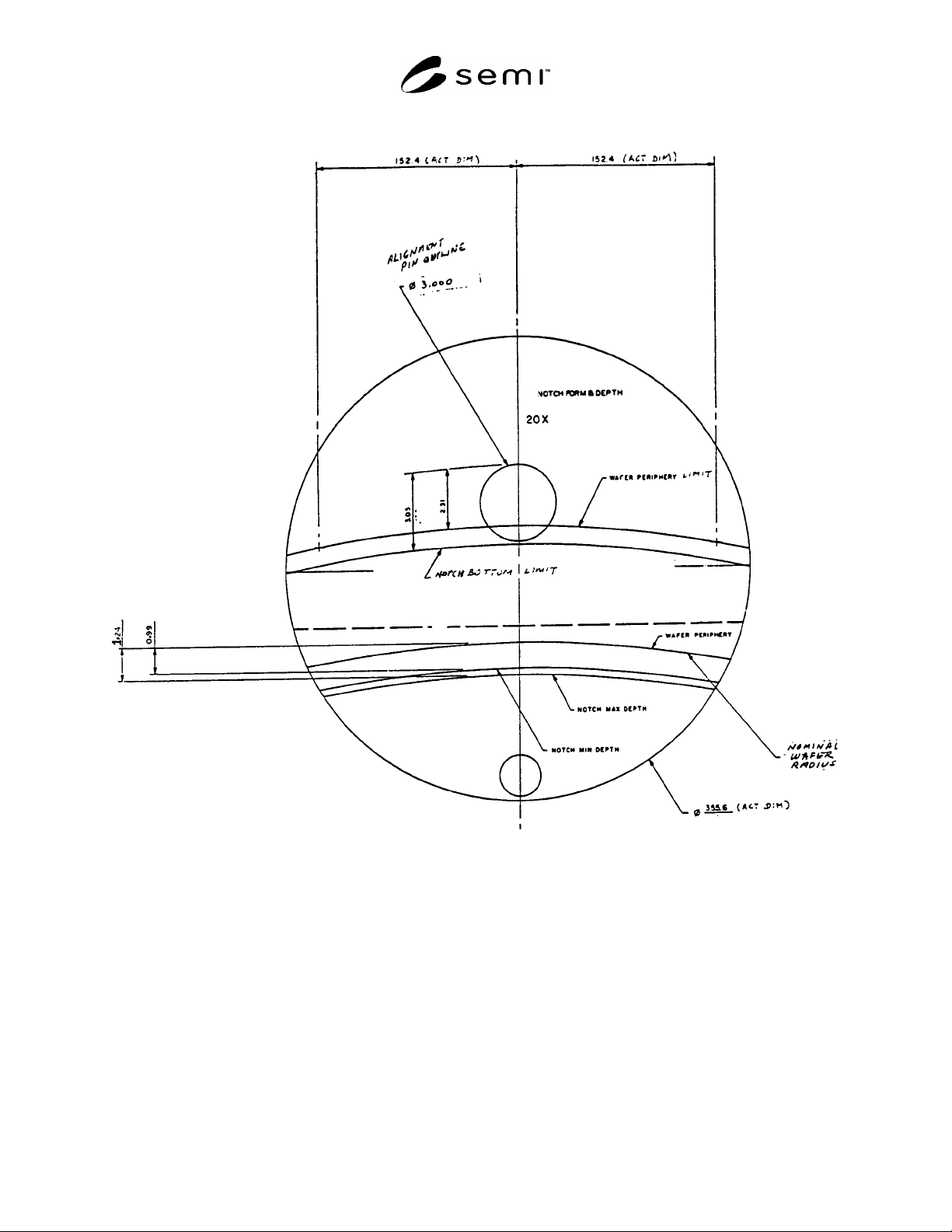
6.3.1 The notch form and depth template has two sections that define (1) the locations of the notch bottom and
wafer periphery relative to the center of the alignment pin, and (2) the location of the notch bottom relative to the
wafer periphery. Separate templates are required for each wafer diameter to be tested. An example of a notch form
and depth template is given in Figure 1.
6.3.2 The notch angle template contains angles from 88° to 96° in 1° increments.
6.3.3 Instructions for constructing templates are given in §9.
6.4 Gage Block or Precision Rod — with dimensions approximately the same as the depth of the notch and
accurately known for use in establishing the magnification of the apparatus.
6.5 Rule — 150 mm long with scale gradations of 0.5 mm or less.
7 Sampling
7.1 Unless otherwise specified, ANSI/ASQC Z1.4 shall be used. Inspection levels shall be agreed upon between
the supplier and purchaser.
8 Determination of Magnification Factor
8.1 Adjust the comparator to the desired magnification. Using the gage block or precision rod of accurately known
dimensions, follow the manufacturer's instructions to establish the object-to-image magnification to three significant
figures.
9 Preparation of Template
9.1 Multiply each of the chosen or specified template dimensions by the magnification factor.
9.2 Prepare on transparent material a full-scale template having the dimensions calculated in ¶9.1 with a projected
image accuracy of ±0.5 mm ( 0.020 in.).
SEMI MF1152-0305 © SEMI 2003, 2005 3
9.3 Include horizontal and vertical axes and label the lines on the notch form and depth template as shown in Figure
1.
NOTE: In use the template is rotated 90° counterclockwise.
Figure 1
Example of Notch Form and Depth Template
10 Procedure
10.1 Set the magnification to 20×.
10.2 Align the fixture in the comparator so that the notch is at the nine o’clock position and the directions of
horizontal and vertical motion of the fixture in the comparator are parallel with and perpendicular to, respectively,
the diameter that passes through the notch.
10.3 Place the notch form and depth template on the comparator screen. Align the horizontal and vertical lines with
the simulated pin outline in the nine o'clock position.
10.4 Place the first wafer to be tested in the fixture, front surface up.

SEMI MF1152-0305 © SEMI 2003, 2005 4
10.5 Align the fixture using only table crossfeed (horizontal) control and fixture rotation so that the simulated pin
outline on the template makes contact with the sides of the notch image.
10.6 Verify that the image of the notch bottom falls on or below the NOTCH BOTTOM LIMIT line. If the image
of the notch bottom falls above this line, record the wafer as defective.
10.7 Verify that the image of the wafer edge falls on or above the WAFER PERIPHERY LIMIT line. If the image
of the wafer edge falls above this line, record the wafer as defective.
10.8 Move the fixture to the right until the image of the wafer edge falls on the line marked WAFER PERIPHERY
using only the table crossfeed control.
10.9 Verify that the notch bottom falls between the NOTCH MAX DEPTH and NOTCH MIN DEPTH lines. If the
image of the notch bottom falls outside these lines, record the wafer as defective.
10.10 Repeat ¶¶10.4 through 10.9 for all remaining wafers to be tested.
10.11 Remove the notch form and depth template and replace it with the notch angle template.
10.12 Set the magnification to 50×.
10.13 Place the first wafer to be tested in the fixture, front surface up.
10.14 Align the image of the wafer notch sides with each angle on the template using the table crossfeed control
and the fixture rotation. Define as the notch angle, the angle that provides the best fit to the image. If the notch
angle is < 89 or > 95°, record the wafer as defective.
10.15 Repeat ¶10.14 for all remaining wafers to be tested.
10.16 On completion of the testing, return the magnification to 20×.
11 Report
11.1 Report as a minimum the following information:
11.1.1 Date of test,
11.1.2 Name of person conducting the test,
11.1.3 The lot number of other identification of the material,
11.1.4 The number of wafers in the lot,
11.1.5 The number of test wafers, and
11.1.6 The number of defective wafers.
11.2 If desired, a table of the types of defects observed may be provided.
12 Precision and Bias
12.1 An interlaboratory evaluation of this test method has not been executed, nor is one anticipated. Use of the test
method for commercial transactions is not recommended unless the parties to the test establish the degree of
correlation that can be obtained.
12.2 A dimension of 0.1 mm in the object plane produces a screen image of 2.0 mm at 20× and of 5.0 mm at 50×.
The smallest size details of the notch contour which can be inspected by this test method are of comparable
dimensions.
13 Keywords
notch; notch dimension; optical comparator; silicon; wafer