semi合集-English.pdf - 第7303页
SEMI MF1152-0305 © SEMI 2003, 2005 2 NOTICE: Unless otherwise indicated, all documents cited shall be the latest published versions. 5 Summary of Test Method 5.1 The wafe r is aligned in position on an optical comparator…

SEMI MF1152-0305 © SEMI 2003, 2005 1
SEMI MF1152-0305
TEST METHODS FOR DIMENSIONS OF NOTCHES ON SILICON
WAFERS
These test methods were technically approved by the Global Silicon Wafer Committee and are the direct
responsibility of the North American Silicon Wafer Committee. Current edition approved for publication by
the North American Regional Standards Committee on November 4, 2004. Initially available at
www.semi.org January 2005; to be published March 2005. Original edition published by ASTM
International as ASTM F 1152-88. Last previous edition SEMI MF1152-02.
1 Purpose
1.1 Wafers must be accurately aligned in various processing equipment during integrated circuit manufacture.
1.2 A notch ground into the edge of the wafer at a specified orientation provides a positive method for such
alignment. The accuracy of the critical dimensions of the notch controls the possible accuracy of the alignment.
1.3 This test method may be used for process control, quality control, and incoming or outgoing inspection.
1.4 Until an index of precision is determined based on an interlaboratory evaluation, this test method is not
recommended for use in decisions between purchasers and suppliers.
2 Scope
2.1 This test method covers a nondestructive procedure to determine whether or not the dimensions, except for the
blend radius, of fiducial notches on silicon wafers fall within specified limits.
2.2 This test method is specifically directed to the notch dimensions specified in SEMI M1, but with suitable
modifications, the principles of this test method may be applied to any desired notch dimensions.
2.3 No test is provided for the blend radius at the apex of the notch.
2.4 The values stated in SI units are to be regarded as the standard. The values given in parentheses are for
information only.
NOTICE: This standard does not purport to address safety issues, if any, associated with its use. It is the
responsibility of the user of this standard to establish appropriate safety and health guides and determine the
applicability of regulatory or other limitations prior to use.
3 Limitations
3.1 Any foreign material or rough spots on the notch edge in the light path may present a distorted image which can
result in the determination of incorrect dimensions.
3.2 Alignment of the notch position with respect to the center of the wafer is important in achieving an accurate
determination of the notch characteristics.
3.3 Wear of grinding tools and process variations may result in notch edges which are not exactly straight and a
nonunique radius at the apex of the notch. Under these conditions, great care must be taken to align the image of the
notch correctly against the appropriate portions of the template.
4 Referenced Standards
4.1 SEMI Standard
SEMI M1 — Specifications for Polished Monocrystalline Silicon Wafers
4.2 ANSI Standard
1
ANSI/ASQC Z1.4 — Sampling Procedures and Tables for Inspection by Attributes
1 American National Standards Institute, New York Office: 25 West 43rd Street, New York, NY 10036, USA. Telephone: 212.642.4900, Fax:
212.398.0023, Website:
www.ansi.org
.

SEMI MF1152-0305 © SEMI 2003, 2005 2
NOTICE: Unless otherwise indicated, all documents cited shall be the latest published versions.
5 Summary of Test Method
5.1 The wafer is aligned in position on an optical comparator and the image of the notch is compared with a series
of templates projected on the screen of the comparator.
5.2 First, the wafer is aligned so that the sides of the image of the notch contact the image of the alignment pin for
fixing the position of the wafer in use. In this case, the image of the notch bottom must lie on or below the
designated line on the notch form/depth template and the image of the wafer edge must lie on or above another
designated line on the template.
5.3 The wafer is then aligned so that the image of the wafer edge coincides with the wafer periphery line on the
template. In this case, the image of the notch bottom must lie between maximum and minimum lines on the
template.
5.4 The image of the notch sides are compared with a series of angles on the notch angle template and the angle that
makes the best fit is chosen as the value of the notch angle.
6 Apparatus
6.1 Optical Comparator — capable of 20× and 50× magnification with a viewing screen large enough to display an
area 5 by 5 mm at 20× or 2 by 2 mm at 50×.
6.2 Fixture — for holding the wafer to be tested. The fixture must provide means for positioning the wafer such
that the plane of the surface of the wafer is perpendicular to the viewing direction and that the wafer can be rotated
about its center. The horizontal and vertical motions are parallel or perpendicular to the diameter of the wafer that
passes through the notch.
6.3 Templates — having lines which define the limits of the notch dimensions. Two templates are required.
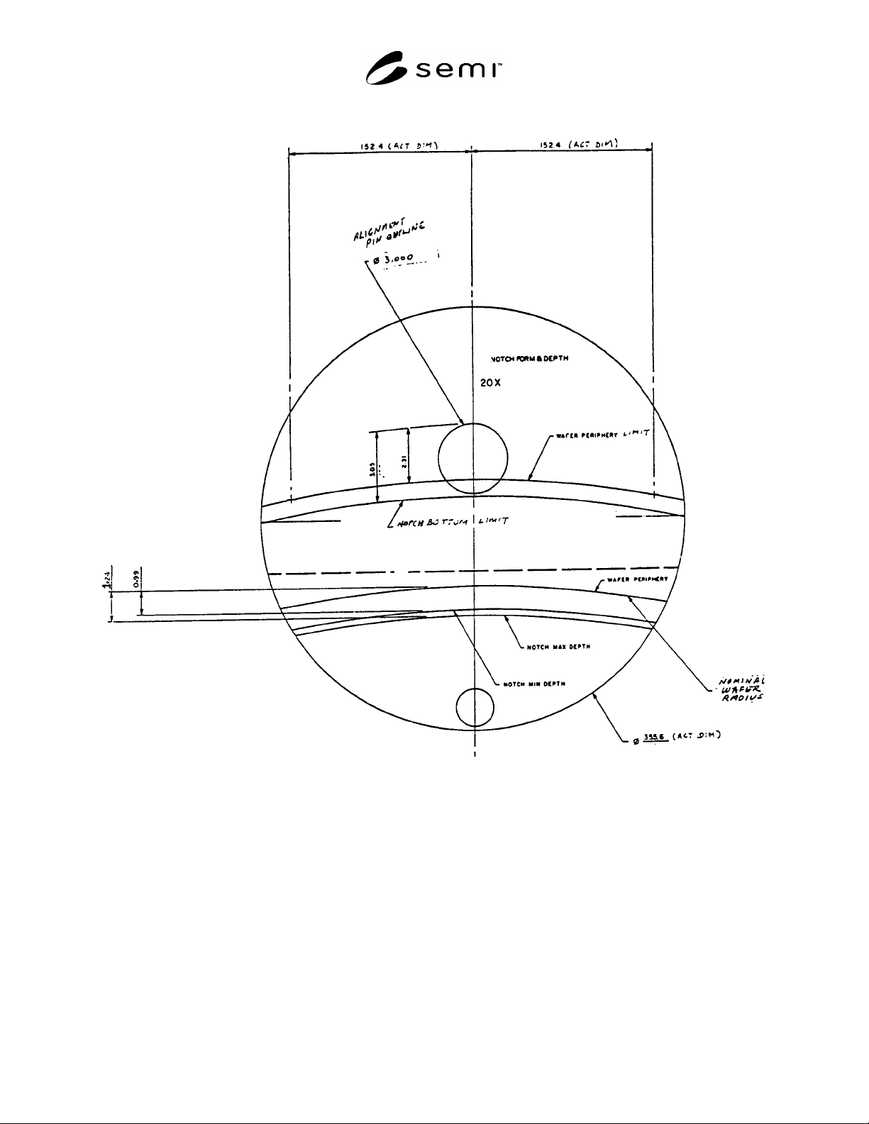
6.3.1 The notch form and depth template has two sections that define (1) the locations of the notch bottom and
wafer periphery relative to the center of the alignment pin, and (2) the location of the notch bottom relative to the
wafer periphery. Separate templates are required for each wafer diameter to be tested. An example of a notch form
and depth template is given in Figure 1.
6.3.2 The notch angle template contains angles from 88° to 96° in 1° increments.
6.3.3 Instructions for constructing templates are given in §9.
6.4 Gage Block or Precision Rod — with dimensions approximately the same as the depth of the notch and
accurately known for use in establishing the magnification of the apparatus.
6.5 Rule — 150 mm long with scale gradations of 0.5 mm or less.
7 Sampling
7.1 Unless otherwise specified, ANSI/ASQC Z1.4 shall be used. Inspection levels shall be agreed upon between
the supplier and purchaser.
8 Determination of Magnification Factor
8.1 Adjust the comparator to the desired magnification. Using the gage block or precision rod of accurately known
dimensions, follow the manufacturer's instructions to establish the object-to-image magnification to three significant
figures.
9 Preparation of Template
9.1 Multiply each of the chosen or specified template dimensions by the magnification factor.
9.2 Prepare on transparent material a full-scale template having the dimensions calculated in ¶9.1 with a projected
image accuracy of ±0.5 mm ( 0.020 in.).
SEMI MF1152-0305 © SEMI 2003, 2005 3
9.3 Include horizontal and vertical axes and label the lines on the notch form and depth template as shown in Figure
1.
NOTE: In use the template is rotated 90° counterclockwise.
Figure 1
Example of Notch Form and Depth Template
10 Procedure
10.1 Set the magnification to 20×.
10.2 Align the fixture in the comparator so that the notch is at the nine o’clock position and the directions of
horizontal and vertical motion of the fixture in the comparator are parallel with and perpendicular to, respectively,
the diameter that passes through the notch.
10.3 Place the notch form and depth template on the comparator screen. Align the horizontal and vertical lines with
the simulated pin outline in the nine o'clock position.
10.4 Place the first wafer to be tested in the fixture, front surface up.