semi合集-English.pdf - 第5993页
SEMI P43-0304 © SEMI 2004 2 SEMI Compilation of Terms 4.2 ISO Standar ds 2 International Vocabulary o f Basic and Ge neral Terms in Metrol ogy 4.3 Other St andards International Techno logy Roadmap for Semiconductors (IT…
SEMI P43-0304 © SEMI 2004 1
SEMI P43-0304
PHOTOMASK QUALIFICATION TERMINOLOGY
This terminology was technically approved by the Global Micropatterning Committee and is the direct
responsibility of the European Micropatterning Committee. Current edition approved by the European
Regional Standards Committee on January 9, 2004. Initially available at www.semi.org February 2004; to be
published March 2004. This document replaces SEMI PR7-0302 in its entirety.
1 Purpose
1.1 This standard defines a unique language in the field
of specification for, and qualification of, photomasks
for use in optical lithography within the semiconductor
industry.
2 Scope
2.1 At present only the International Technology
Roadmap for Semiconductors (ITRS) serves as a
universally accepted working document on how to
specify photomasks, however the definitions used are
subject to interpretation. Different tool makers, mask
makers and mask users are hindered in the
communication with each other, as they first need to
know and understand each others terminology. The
lack of a common terminology complicates comparison
of tools. A uniformly used, and universally accepted
terminology, with a minimum of ambiguity, is required.
2.2 The definitions listed are for mask qualification,
incorporating 3 possible types of value for a given
qualification parameter:
• <(true) qualification parameter>, which would be
the result of an ideal measurement of the total
population of features of interest
1
.
• <measured qualification parameter>, the result of
a given population of measurements. It is hereby
mentioned that a measured value (for example the
mean, the standard deviation, the range) is always
subject to the sample size of the measured
population and the measurement method.
Therefore both the sample size and the
measurement method are mandatory information.
• <qualification parameter spec(ification)>, the
maximum or minimum value that may not be
exceeded for the selected population of
measurements which must be defined as mandatory
information.
2.2.1 The first two types of value for a given
parameter, the true and measured qualification
parameters, will be defined in the present document.
1 See reference document in Section 4.2.
2.2.2 The third parameter type, the parameter
specification, will not be discussed here, since it is
subject to the agreement between the individual parties
of the mask qualification process.
2.3 In order to assist users, the major differences in
recommended default values between this standard and
the ITRS mask table definitions are noted where
applicable.
NOTICE: This standard does not purport to address
safety issues, if any, associated with its use. It is the
responsibility of the users of this standard to establish
appropriate safety and health practices and determine
the applicability of regulatory or other limitations prior
to use.
3 Limitations
3.1 This document is restricted to dimensional
metrology aspects. Other conventional mask
qualification aspects, including those related to
materials, overlay and defectivity, are not considered
within the scope of this version.
3.2 The definitions listed are specific to state-of-the-art
photomasks, with a focus on reduction reticles. They
may therefore overrule any related terminology in other
standards, with a more general scope. Application to
other types of masks, e.g., for next generation
lithography, may be feasible, but is not within the scope
of the present document.
4 Referenced Standards
4.1 SEMI Standards
SEMI P10 — Specification of Data Structures for
Photomask Orders
SEMI P19 — Specification for Metrology Pattern Cells
for Integrated Circuit Manufacture
SEMI P21 — Guidelines for Precision and Accuracy
Expression For Mask Writing Equipment
SEMI P22 — Guideline for Photomask Defect
Classification and Size Definition
SEMI P24 — CD Metrology Procedures
SEMI P35 — Terminology for Microlithography
Metrology
SEMI P43-0304 © SEMI 2004 2
SEMI Compilation of Terms
4.2 ISO Standards
2
International Vocabulary of Basic and General Terms
in Metrology
4.3 Other Standards
International Technology Roadmap for Semiconductors
(ITRS)
3
NOTICE: Unless otherwise indicated, all documents
cited shall be the latest published versions.
5 Interpretation of Related General
Terminology
NOTE 1: This paragraph includes general terms, as a basis
for the specific mask related terminology, which is the main
subject of this document.
5.1 feature — as defined in SEMI P35.
5.2 proximity range — distance over which a feature
influences another significantly (criterion to be stated).
This term applies to mask fabrication, mask metrology
and/or printed wafer image, defining 3 types of
proximity range (for example mask fabrication
proximity range). It is mandatory to state which of the
3 types is referred to.
NOTE 2: Within this document proximity range will refer by
DEFAULT to the first type mentioned.
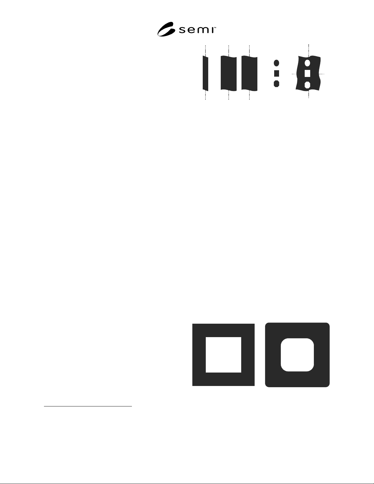
5.3 line — a clear field, dark feature of quasi-infinite
length (>> proximity range) determined by its width. A
line is an example of a 1D feature (see Figure 1).
5.4 space — in analogy to line, but a clear feature in a
dark field (see Figure 1).
5.5 contact — a clear feature in a dark field with
length:width ratio ranging from 0.5 (1 is default) to 2
maximum (see Figure 1). The width of such feature
may be measured as if it were a 1D feature, but for
enhanced relevance it requires 2D assessment such as
an area measurement. A large contact can be called a
window.
5.6 dot — in analogy to contact, but a dark feature in a
clear field (see Figure 1). A large dot can be called a
pad.
5.7 isolated feature — feature that has no neighbors
that are within a distance smaller than the proximity
range to any edge of the feature.
2 International Organization for Standardization 1, rue de Varembé
Case Postale 56 CH-1211 Genève 20 Switzerland
3 International Technology Roadmap for Semiconductors, organized
by International SEMATECH, 2706 Montopolis Drive, Austin, Texas
78741, see itrs.org
line space dots contacts
Figure 1
Nomenclature for Feature Types (as Designed)
Default contact (dot) is square.
5.8 dense features — features that influence each other
(i.e., features that are not isolated). Clarification is
required to describe the proximity, either by detailing
the feature pitch and number of lines, for regular arrays
(pitch = design values of line width and space width
added), or by describing the surrounding area (see
Section 7). In absence of such clarification dense is
regarded by default as equal lines and spaces in a semi-
infinite array size, insofar that the feature width does
not exceed the proximity range.
5.9 nominal feature — feature as it is
intended. This
usually corresponds to the data used for mask making,
including any pre-compensation to overcome process
biases of the wafer process (e.g., subresolution features
such as hammerheads and serifs), but excluding any
pre-compensation that is purely done to deal with mask
process limitations (e.g., chrome etch bias). In the
simplest case it corresponds to the original design itself.
5.10 actual feature — feature as it is on the mask. In
practical cases this will include deviations in feature
widths, lengths, shape and position from the nominal
feature.
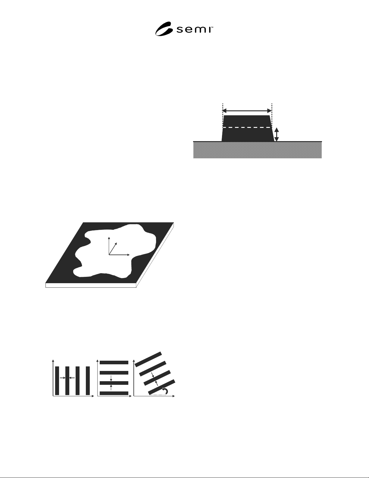
NOTE 3: A feature, whether actual or nominal, may contain
holes, as shown in Figure 2.
Figure 2
Example of Features Containing Holes
(left: nominal; right: actual)
5.11 pattern — subset of a layout containing one or
more features.
SEMI P43-0304 © SEMI 2004 3
NOTE 4: It is possible that some features are only included in
part, see clipped feature.
5.12 region of interest (ROI) — circumscribed section
of a pattern that contains (parts of) the features
considered for measurement.
NOTE 5: It is recommended to make the ROI as small as
possible without affecting the obtained result.
5.13 clipped (nominal/actual) feature — the part of the
(nominal/actual) feature lying within the region of
interest (Figure 7).
5.14 feature (or Pattern) alignment — positioning of
nominal and actual feature (or pattern) relative to each-
other (see Section 8.4).
6 Coordinate System
6.1 The coordinate system XYZ for this document is
defined in Figure 3. It is defined with patterned mask
side upwards and mask orientation as it was patterned.
XY determines the mask plane. Z is the direction
perpendicular to it. z = 0 at the absorber–substrate
interface and z < 0 to the substrate side. Absorber is for
example chrome or embedded material. (x,y) = (0,0) is
tool or application specific.
X
Y
Z
Figure 3
Mask Coordinate System
6.2 Features are called vertical when their length is
along Y. Feature width is then measured in X. This
corresponds to Figure 2 of SEMI P35. Horizontal
features have their length along X. Feature width is
then measured in Y. See Figure 4.
vertical
X
Y
horizontal
X
Y
other angle
X
Y
+
Figure 4
Orientation of Mask Features
7 1D Mask Qualification Terminology
7.1 feature width — width of a cross section of a mask
feature at a certain height defined by an appropriate
bounding box model as described in SEMI P35 (see
Figure 5). The bounding box model must be stated as
mandatory information, as well as the z height of the
measurement. DEFAULT is at z = 0.
width
height
Figure 5
Cross Section of a Mask Feature
7.2 measured feature width — width determined from
the measured signal obtained on the mask feature. For
example, the width may be determined at a certain level
of the measured signal. To be stated as mandatory
information:
• region of interest. For 1D features this corresponds
to the specified line segment (SEMI P35),
• measurement method used (SEM, optical
reflection, optical transmission, AFM, etc.),
• calibration and/or correlation used,
• precision (SEMI P24),
and as optional information:
• measurement tool (vendor, model or any tool
specific options), and
• measurement algorithm used.
NOTE 6: The bounding box could be infinitely short as in the
special situation of a measurement of a feature using a cross-
section.
7.3 feature width deviation (from target) — difference
between actual and nominal feature width.
7.4 measured feature width deviation (from target) —
difference between measured and nominal feature
width.
7.5 feature edge — position of the material boundary
of a mask feature at a certain height of the physical
cross section (see Figure 2 of SEMI P35), to be stated
as mandatory information. DEFAULT is
feature/substrate interface.