semi合集-English.pdf - 第7438页
9.2.5 More complex calculations may al so be used to determine acceptability. For exam ple, a histogram of the parameter values of the DDS along with statistical measures (mean, sample stan dar d deviation, etc.) may be …
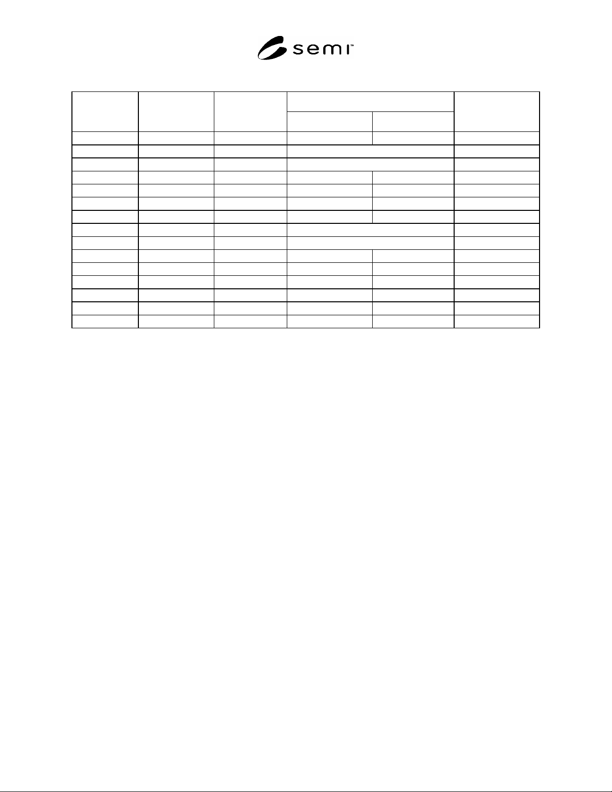
Table 1 Acronyms for Wafer Flatness Parameters
Reference Plane
Acronym
Measurement
Method
Reference Surface
Construction Area
Measurement
Parameter
GBIR Global Back Ideal back surface Entire FQA Range (TIR)
GF3R Global Front Three-point Range (TIR)
GF3D Global Front Three-point Deviation (FPD)
GFLR Global Front Least squares Entire FQA Range (TIR)
GFLD Global Front Least squares Entire FQA Deviation (FPD)
SBIR Site Back Ideal back surface Entire FQA Range (TIR)
SBID Site Back Ideal back surface Entire FQA Deviation (FPD)
SF3R Site Front Three-point Range (TIR)
SF3D Site Front Three-point Deviation (FPD)
SFLR Site Front Least squares Entire FQA Range (TIR)
SFLD Site Front Least squares Entire FQA Deviation (FPD)
SFQR Site Front Least squares Site Range (TIR)
SFQD Site Front Least squares Site Deviation (FPD)
SFSR Site Front Least squares Sub-site Range (TIR)
SFSD Site Front Least squares Sub-site Deviation (FPD)
8 Materials
8.1 Set-up Masters — suitable to accomplish
calibration and standardization as recommended by the
equipment manufacturer.
8.2 Reference Wafer — with total thickness variation
(TTV) value and flatness value similar to the product or
process to be monitored and with a data set that is used
to determine the level of agreement between the data
set obtained by the measuring equipment under test and
the reference wafer data set (see Section 9 ).
9 Suitability of Measuring Equipment
9.1 Determine the suitability of the measuring
equipment with the use of a reference wafer and its
associated data set in accordance with the procedures of
Sub-section 9.2 , or by performance of a statistically-
based instrument repeatability study to ascertain
whether the equipment is operating within the
manufacturer's stated specification for repeatability.
9.1.1 The reference wafer data set is a set of thickness
or flatness parameters based on corrected data in that all
possible interferences have been removed and the data
has been replanarized in accordance with this method.
9.1.2 Each reference wafer (artifact) is accompanied by
its own data set, the reference data set (RDS), in which
each parameter value is the average of a number of
values obtained for that parameter over a number of
“passes” (repeat measurements). The artifact is
measured on a measurement equipment under test and
its RDS is compared against the resultant-measured
sample data set. Delta-parameter and other values are
computed from the differences. The parameter used to
determine agreement between the artifact and the
measuring equipment under test and the acceptable
level of this agreement is to be agreed upon between the
parties to the test.
9.2 Procedure
9.2.1 Select a reference wafer of appropriate criteria
together with its associated reference data set (RDS).
9.2.2 Measure the reference wafer on the measurement
equipment under test to obtain a sample data set (SDS).
9.2.3 Subtract the two data sets on a parameter basis to
obtain a difference data set (DDS):
DDSSDSRDS
(1)
9.2.3.1 The DDS represents the differences between
the measurements made on the measuring equipment
under test and the reference data set. The DDS contains
many values.
9.2.4 The simplest metric that can be used to determine
acceptability is maximum difference, the largest
absolute value in the DDS. This represents the worst-
case disagreement between the results obtained from
the measurement equipment under test and the
reference data. Accept the measurement equipment as
suitable for measurement if the maximum difference is
less than a value that is agreed upon between the parties
to the test.
SEMI MF1530-1104 © SEMI 2003, 2004 3

9.2.5 More complex calculations may also be used to
determine acceptability. For example, a histogram of
the parameter values of the DDS along with statistical
measures (mean, sample standard deviation, etc.) may
be used. These measures may be compared to
application-specific limits or used to provide insight
into the nature and source of the difference, or both, as
arranged by agreement of the parties to the test.
10 Sampling
10.1 This test method is nondestructive and may be
used on either 100% of the wafers in a lot or on a
sampling basis.
10.1.1 If samples are to be taken, procedures for
selecting the sample from each lot of wafers to be tested
shall be agreed upon between the parties to the test, as
shall the definition of what constitutes a lot.
11 Calibration and Standardization
11.1 Calibrate the measuring equipment in accordance
with the manufacturer's instructions.
12 Procedure
12.1 Prepare the apparatus for measurement of wafers,
including selection of data display/output functions.
12.2 Select the fixed quality area (FQA) by specifying
the nominal edge exclusion EE.
12.3 Select the flatness parameter(s) to be determined
as follows:
12.3.1 Select the measurement method — global
flatness (G) or site flatness (S):
12.3.1.1 If S is chosen, then also specify site array
details:
12.3.1.1.1 site size,
12.3.1.1.2 location of sites relative to FQA center,
12.3.1.1.3 location of sites relative to each other,
rectilinear or tiled pattern, and
12.3.1.1.4 partial sites, included or excluded.
12.3.2 Select the reference surface — front (F) or back
(B).
12.3.3 Select the reference plane construction and area
as follows:
12.3.3.1 For global flatness measurements, select one
of the following global reference planes using all points
within the FQA to construct the reference plane:
12.3.3.1.1 Ideal back surface plane (I),
12.3.3.1.2 Three-point front surface plane (3), or
12.3.3.1.3 Least-squares front surface plane (L).
12.3.3.2 For site flatness measurements with a global
reference plane, select one of the following global
reference planes using all points within the FQA to
construct the reference plane:
12.3.3.2.1 Ideal back surface plane (I),
12.3.3.2.2
Three-point front surface plane (3), or
12.3.3.2.3 Least-squares front surface plane(L).
12.3.3.3 For site flatness measurements with a site
reference plane, select the following reference plane
using all points within the site that lie within the FQA
to construct the reference plane:
12.3.3.3.1 Site least-squares front surface plane (Q).
12.3.3.4 For scanner site flatness measurements with a
sub-site reference plane, select the following reference
plane using all points within the sub-site that lie within
the FQA to construct the reference plane:
12.3.3.4.1 Sub-site least squares front surface plane
(S).
12.3.4 Select the measurement parameter:
12.3.4.1 Global Flatness:
12.3.4.1.1 Range (Total indicator reading, TIR) (R), or
12.3.4.1.2 Deviation (Focal plane deviation, FPD) (D).
12.3.4.2 Site Flatness:
12.3.4.2.1 Range (TIR) — each site or maximum value
for all sites, or both, or
12.3.4.2.2 Deviation (FPD) — each site or maximum
value for all sites, or both, or
12.3.4.2.3 A map or histogram showing the
distribution of either or both of these values.
12.4 Introduce the test specimen into the measurement
mechanism and initiate the measurement sequence.
12.5 Use the resulting data set, whose elements are the
thicknesses [t(x,y)] as the basis to make thickness and
flatness calculations.
13 Calculations
13.1 The calculations of wafer thickness, total
thickness variation and the desired flatness parameter(s)
are performed automatically within the instrument. An
outline of the calculation structures is provided here to
indicate the nature of the procedure.
13.2 Thickness Determination
13.2.1 Determine the displacements (distances)
between each probe and the nearest surface of the wafer
SEMI MF1530-1104 © SEMI 2003, 2004 4

(in pairs) at intervals along the scan pattern. At each
measurement location, the sum of the displacements is
subtracted from D, yielding the thickness at each
measurement location as follows:
(2)
)],(),([),(),( yxbyxayxDyxt
where:
D = distance between Probes A and B,
a = distance between Probe A and the nearest
wafer surface,
b = distance between Probe B and the nearest
wafer surface, and
t = wafer thickness (see Figure 1).
13.2.2 Take the wafer thickness as the thickness at the
center point of the wafer.
13.2.3 Determine the total thickness variation, TTV, as
the largest thickness value, t
max
minus the smallest
thickness value, t
min
:
(3)
minmax
ttTTV
13.3 Flatness Determination
13.3.1 Construct the reference plane from the data set
t(x,y). The reference plane is of the following form (see
Notes 2 and 3):
(4)
RRRref
cybxaZ
where a
R
, b
R
, and c
R
are constants chosen as follows:
13.3.1.1 For ideal back surface reference plane,
(5) 0
RRR
cba
13.3.1.2 For the least squares reference plane, select
a
R
, b
R
, and c
R
so that (see Note 4):
(6)
yx
RRR
cybxayxt
,
2
)](),([
is minimized over the FQA for global determination,
over the portion of the site within the FQA for site
determination, or over the portion of the sub-site within
the FQA for sub-site determination.
13.3.1.3 For the three-point reference plane, construct
a plane so that
(7)
RRR
RRR
RRR
cybxayxt
cybxayxt
cybxayxt
3333
2222
1111
),(
and,),(
,),(
where x
1
, y
1
; x
2
y
2
; and x
3
, y
3
are equally spaced points
located on a circle whose perimeter is located 3 mm
from the edge of a wafer of nominal diameter (see Note
4).
13.3.2 Construct a focal plane to calculate deviation
parameters from the data set t(x,y). The focal plane is
of the following form:
FFFfocal
cybxaZ
(8)
The focal plane is parallel with the reference plane so
that in all cases
a
F
= a
R
, and
b
F
= b
R
.
13.3.2.1 A global focal plane is the same as the
corresponding reference plane so that
c
F
= c
R
.
13.3.2.2 A site or sub-site focal plane is displaced from
the corresponding reference plane as follows:
c
F
= t(x
0
,y
0
) (a
F
x
0
+ b
F
y
0
)
where x
0
and y
0
are the coordinates of the site or sub-
site center, respectively.
NOTE 2: Use of the thickness data set, t(x,y), in this regard is
equivalent to setting the origin of the z-axis, as defined in
SEMI M20, at the back surface of the wafer at each point of
the data set. Then the value of z at each point is equal to the
thickness t at that point. This is equivalent to constraining the
wafer so that the back surface is pulled down uniformly onto
an ideal chuck.
NOTE 3: The constants a
R
and a
F
provide the slopes of the
reference and focal planes, respectively, in the x direction, the
constants b
R
and b
F
provide the slopes of the reference and
focal planes, respectively, in the y direction, and the constants
c
R
and c
F
provide the distances of the center point of the
reference and focal planes, respectively, from the back surface
at that point.
NOTE 4: The values t(x,y) at any point represent z
f
(x,y),
where z
f
is the height of the front surface from the z-axis
origin at each point. It is use of this data set that causes the
reference surface to be the front surface for both the least
squares and three-point reference planes.
13.3.3 Determine the point-by-point differences
between the thickness and the reference or focal plane
by
)(),(),(
iii
cxbxayxtyxf
(9)
where the subscript i is either R or F depending on
whether a reference or focal plane is being used and x
and y range over the FQA, the site, or the sub-site, for
global, site, or sub-site determinations.
13.3.4 Determine range (also called TIR) as follows:
minmax
),(),( yxfyxfTIR
(10)
where:
f
(x,y)
max
= largest (most positive) algebraic value of
SEMI MF1530-1104 © SEMI 2003, 2004 5