semi合集-English.pdf - 第5185页
SEMI M34-0299 © SEMI 1999 3 7.1.2 S pectroscopic Ellipso metry Measurement — In this measurement, white light from a xenon arc lamp passes through a polarizing rotating filter and illuminates the sample site under study;…
SEMI M34-0299 © SEMI 1999 2
7. Test Methods - Dimensions
7.1 SIMOX Layer Thickness Measurements
7.1.1 Measurements Methods Two non-contact,
non-destructive optical characterization techniques,
spectroscopic reflectometry and spectroscopic
ellipsometry, have proven useful for SIMOX layer
thickness measurements. Both techniques use reflected
light to allow deduction of the thickness and refractive
index of thin film layers. In both cases, film thickness
and index of refraction data must be " backed out" of the
measured optical data by a process of successive
approximation. In both cases, the fitting procedure is
more straightforward and more accurate the as-annealed
SIMOX wafers with abrupt silicon/oxide interfaces than
for the implanted SIMOX wafers with extended
interface zones. Silicon islands and interface
nonuniformities make these techniques problematic for
SIMOX wafers with oxygen implant doses below the
" stoichiometric dose" , roughly 1.6 × 10
18
O
+
/cm
2
for a
375 nm oxide layer.
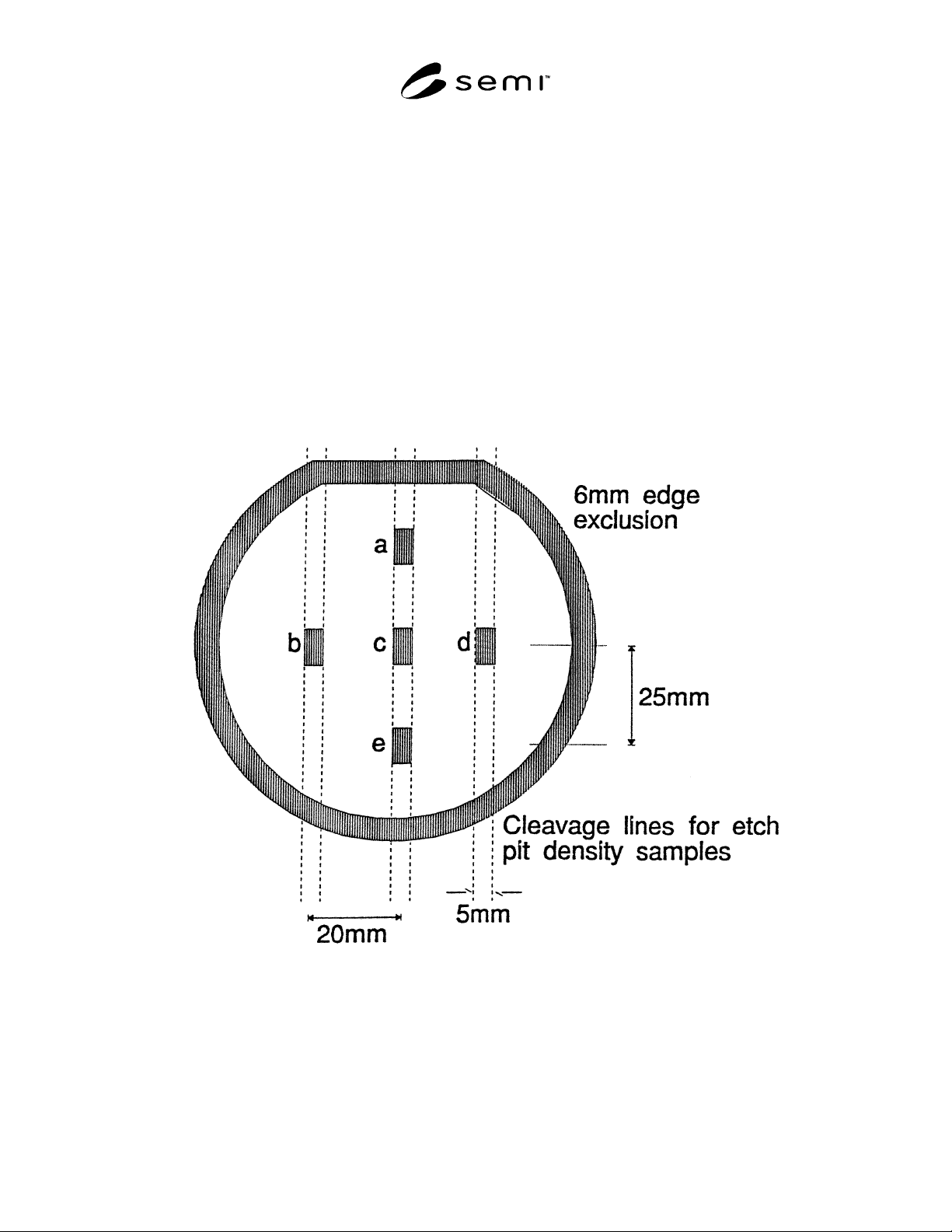
7.1.1.1 The measurement strategy is to make a detailed
measurement with an accurate fit on at least five wafer
sites, including the center as illustrated in Figure 1. The
number of wafer sites to be monitored should be agreed
on between customer and vendor. Generally, the greater
the variability relative to the mean, the larger the
number of sites that should be monitored. In each case,
the measurement system supplies a " goodness-of-fit"
parameter which indicates a level of confidence in the
fit to the measured data.
Figure 1
Schematic of Measurement Sites, Cleavage Lines, and Edge Exclusion for 100 mm SIMOX Wafer Inspection

SEMI M34-0299 © SEMI 1999 3
7.1.2 Spectroscopic Ellipsometry Measurement — In
this measurement, white light from a xenon arc lamp
passes through a polarizing rotating filter and
illuminates the sample site under study; reflected light
passes through an analyzer to a monochromator and
photomultiplier detector. For each wavelength,
reflectivity oscillates with polarizer rotation; the
magnitude and phase of reflectivity changes are
measured to determine ellipsometric angles, δ and ψ.
The two measured spectra are fit by successive
approximation to allow determination of the silicon and
oxide layer thickness and oxide composition.
Ellipsometry measurements are only specified for the
annealed SIMOX wafers. For spectroscopic
ellipsometry, the choice of instrument and associated
model and fitting parameters affect the confidence-of-
fit, so they should be taken into account in the
user/supplier agreement. For example, with the SOPRA
SE system, the goodness-of-fit error estimator shall be
less than 0.025 for accurate structural models.
7.1.3 Optical Reflectance Measurements — In this
measurement, light from a xenon arc lamp passes
through a grating monochromator and illuminates the
sample site under study; reflected light is gathered by
an intrinsic silicon detector. Specular reflectivity is
plotted as a function of wavelength from 0.4 micron to
1.1 micron. The analysis proceeds by making
successively better approximations to the oxygen
content, index of refraction, and absorption of each
layer until an acceptable fit is achieved. Measurements
are made with a reflectance mode optical
interferometer.
7.1.4 Optical Model Fitting and Correlation — There
are slight, systematic differences between layer
thickness measured by reflectance and by spectroscopic
ellipsometry (SE). Because of this, user and supplier
should specify the actual measurement method to be
used. The two methods offer results which are
reproducible and well-correlated with each other over a
wide range of conditions. If both measurement
techniques are used, it is recommended that the
reflectance system measurements be calibrated to fit the
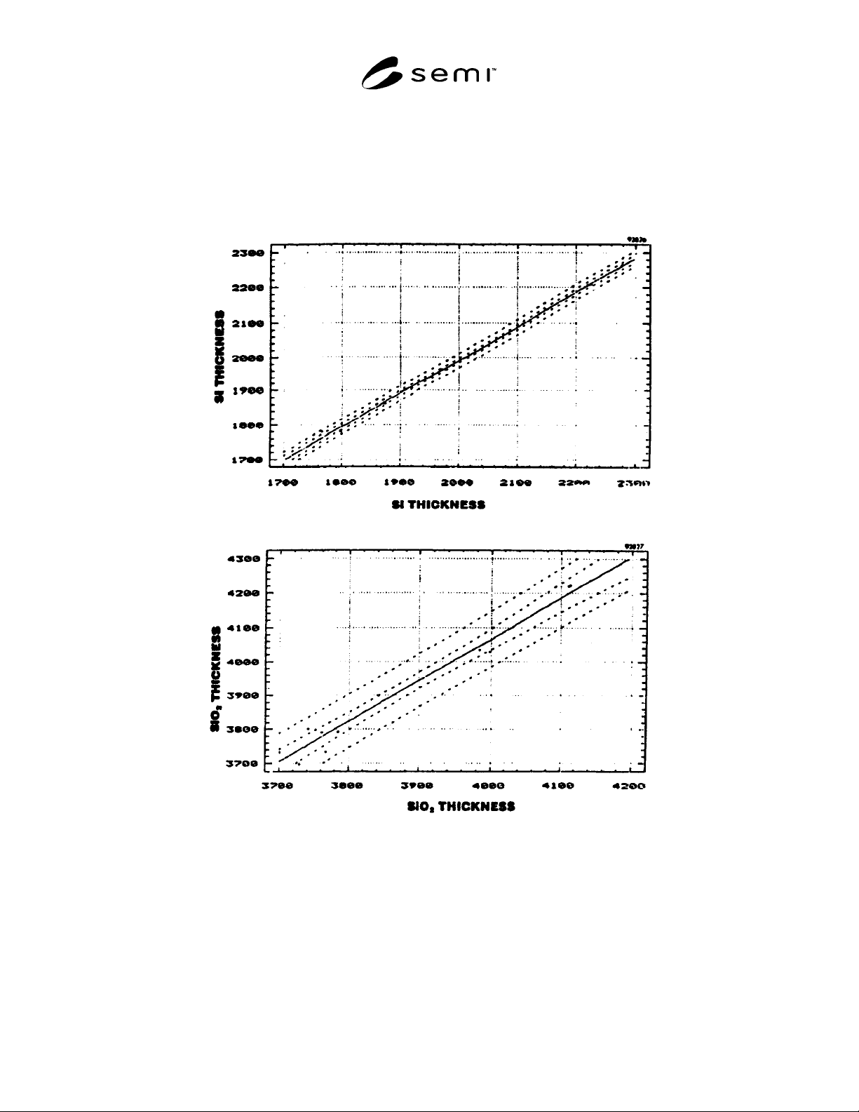
results of the SE. Figure 2 shows conversion curves for
top silicon and oxide layer thickness measurements
made with the two measurement techniques.
7.1.5 Top Silicon Layer Thickness — See Section
7.1.4 on correlation of reflectance and spectroscopic
ellipsometry (SE) measurements. Optical measure-
ments will be made on five wafer sites as shown in
Figure 1. Spectra for each site will be fit independently
with both the top silicon and oxide layer thickness as
adjustable parameters. Both the mean thickness and the
uniformity should be specified. Depending on the type
of SIMOX wafer being specified, the mean thickness of
the top silicon layer will be from 50 nm to 500 nm.
Following is an example specification: Mean top silicon
layer thickness for the five sites will be 215 ± 10 nm
with acceptable goodness-of-fit at all five sites. Top
silicon non-uniformity will be less than ± 5 nm.
7.1.6 Buried Oxide Layer Thickness — See Section
7.1.4 on correlation of reflectance and spectroscopic
ellipsometry (SE) measurements. Optical measure-
ments will be made on five wafer sites as shown in
Figure 1. Spectra for each site will be fit independently
with both the top silicon and the buried oxide layer
thickness as adjustable parameters. Both the mean
thickness and the uniformity should be specified.
Depending on the type of SIMOX wafer being
specified, the mean thickness of the buried oxide layer
is from 50 nm to 500 nm. Following is an example
specification: Mean buried oxide layer thickness for the
five sites will be 380 nm ± 20 nm with acceptable
goodness-of-fit at all five sites. Buried oxide uniformity
will be less than ± 10 nm.
7.2 Crystallographic Defect Measurements - Test
Methods — The evaluation of threading dislocation
density in the top SI layer will be made by destructive
chemical etching and microscopic etch pit density
measurements. The appropriate evaluation procedure
for given SIMOX wafer, which depends on the
threading dislocation density and the thickness of top Si
and buried oxide layers, will be determined by the
agreement between user and supplier.
7.2.1 Optionally, other crystallographic defects which
may be formed in the top Si layer of SIMOX wafers,
such as oxide precipitates or micro stacking faults,
silicon crystal defects induced by surface particles prior
to epi growth when epi is used to increase the thickness
of the top silicon. A sampling plan should be
established based on experience with the supplier.
7.2.2 Following are examples of the evaluation of
threading dislocations in two kinds of SIMOX wafers:
7.2.2.1 Example 1. Threading dislocation evaluation in
SIMOX wafers with 200 nm thick top Si layer and 400
nm thick buried oxide: Samples are handled with plastic
tweezers throughout the etching procedure. Samples are
first stripped of native oxide by dipping in Bell 2 or HF
stripping solutions. Immediately after stripping, wafers
are dipped in freshly prepared standard Secco Etch: one
part (by volume) of a 0.15 molar solution of K
2
Cr
3
O
7
in
distilled water and two parts HF (49%). Samples are
dipped in the Secco etch until 50 nm of silicon remains,
and then they are rinsed thoroughly in distilled water
and blown dry. The thickness of the remaining silicon
ensures that stacking fault pyramids found in multiple
implant material are counted. The threading dislocation
density may vary over a wide range, depending on the
SEMI M34-0299 © SEMI 1999 4
type of material. The Secco Etch, as described, creates
etch pits that appear as dark circles roughly 50 nm in
diameter, and pictures should be taken at 2500X to
20,000X magnification in order to unambiguaously
identify and count the etch pits. This is suitable for high
density defect samples. For lower dislocation densities
typical of recent SIMOX material, a third etch in
buffered HF (1 HF (49%): 6 NH
4
F (40%)) for 10
minutes will etch the buried oxide under each Secco
etch pit, creating a char-acteristic circular shape 2 µm
in diameter that can be seen at 500X magnification.
Figure 2
Calibration Curves Relating Reflectance Measurements to Ellipsometry Measurements for Top Silicon and
Buried Oxide Layer Thickness
NOTE: Dashed lines are at ± 1 sigma and ± 3 sigma.