semi合集-English.pdf - 第5216页
SEMI M39-0999 © SE MI 1999 2 capable of m ea suring the specimen thickness within ± 1% must be used. 7.2 Magnet A calibrated magne t ca pable o f providin g a magn etic f l ux den sity uniform with i n ± 1% over th e a…

SEMI M39-0999 © SEMI 19991
SEMI M39-0999
TEST METHOD FOR MEASURING RESISTIVITY AND HALL
COEFFICIENT AND DETERMINING HALL MOBILITY IN SEMI-
INSULATING GaAs SINGLE CRYSTALS
This test method was technically approved by the Global Compound Semiconductor Committee and is the
direct responsibility of the Japanese Compound Semiconductor Committee. Current edition approved by the
Japanese Regional Standards Committee on June 1, 1999. Initially available at www.semi.org August 1999;
to be published September 1999.
1 Purpose
1.1 The purpose of this document is to specify a meth-
od to measure resistivity and determine Hall mobility of
semi-insulating GaAs single crystals by the Van der
Pauw method. Especially, this document specifies a
simple and practical method for commercial semi-
insulating GaAs single crystals.
2 Scope
2.1 This test method covers a procedure for measuring
the resistivity and determining Hall mobility of semi-
insulating GaAs single crystals by the van der Pauw
method. This method requires a singly connected test
specimen without any isolated holes, of homogeneous
thickness and with a square shape. In this method,
contacts must be sufficiently small and located at the
corners of the specimen.
2.2 This standard may involve hazardous materials,
operation, and equipment. This standard does not
purport to address all of the safety problems associated
with its use. It is the responsibility of the user of this
standard to establish appropriate safety and health
practices and determine the applicability of regulatory
limitations prior to use.
3 Referenced Standards
3.1 ASTM Standards
F 76-73 Standard Method for Measuring Hall
Mobility and Hall Coefficient in Extrinsic
Semiconductor Single Crystals
F 76-86 Standard Test Methods for Measuring
Resistivity and Hall Coefficient and Determining Hall
Mobility in Single-Crystal Semiconductors
F 43-93 Standard Test Methods for Resistivity of
Semiconductor Materials
NOTE 1: As listed or revised, all documents cited shall be the
latest publications of adopted standards.
4 Terminology
NOTE 2: Many of the terms associated with this test method
can be found in ASTM Definitions F 76-86.
hall mobility the ratio of the magnitude of the Hall
coefficient to the resistivity; it is readily interpreted
only in a system with carriers of one charge type.
resistivity the ratio of the potential gradient parallel
to the current in the material to the current density. For
the purpose of this method, the resistivity shall always
be determined for the case of zero magnetic flux.
5 Summary of Test Method
5.1 In this method, the thickness of a specimen cut
from a semi-insulating GaAs single crystal is measured.
5.2 Ohmic contacts are formed on the specimen.
5.3 The temperature near the specimen is measured.
5.4 Hall-effect measurement is performed and data are
taken.
5.5 From the measured data, the resistivity and Hall
mobility are calculated and corrected for temperature.
6 Interferences
6.1 Light could cause an error due to photo-
conductivity, so the specimen must be placed in a dark
environment.
6.2 Temperature fluctuation gives significant error.
Specimen itself could be at higher temperature than the
environment if one does not take sufficient time after
soldering the contacts.
6.3 The current-voltage conditions must be ohmic.
6.4 The damaged layer due to the sawing must be
removed by etching the specimen, for example by using
mixture of sulfuric acid (H
2
SO
4
), hydrogen peroxide
(H
2
O
2
) and water (H
2
SO
4
:H
2
O
2
:H
2
O = 3:1:1).
7 Apparatus
7.1 Measurement of Specimen Thickness — Dial
gauge, micrometer, or electronic thickness gauge

SEMI M39-0999 © SEMI 1999 2
capable of measuring the specimen thickness within ±
1% must be used.
7.2 Magnet A calibrated magnet capable of
providing a magnetic flux density uniform within ± 1%
over the area in which the test specimen is to be
located. Flux densities must be between 3,000−10,000
gauss (0.3T−1.0T).
7.3 Instrumentation
7.3.1 Current Source Capable of maintaining
current through the specimen constant to ± 1% during
the measurement. The current source is accurate to ±
1% on all ranges used in the measurement.
7.3.2 Electrometer or Voltmeter With which
voltage measurements can be made to an accuracy of ±
1%. The input resistance of the electrometer (or
voltmeter) must be greater than 1E13 Ω . In addition to
the Electrometer, the input resistance greater than 1E13
Ω must be kept in the Hall measurement system.
7.4 Specimen Holder
7.4.1 Container Used to hold the specimen, to
isolate it from surroundings and shield it from light.
7.4.2 Thermometer Located in close proximity to
the test specimen and associated instruments for
monitoring temperature to an accuracy of ± 0.1°C
during the measurement. This may include, for
example, a thermocouple.
8 Reagents and Materials
8.1 Purity of Reagents All chemicals for which
such specifications exist shall conform to SEMI C1.
8.2 Purity of Water When water is used, it is either
distilled water or deionized water having a resistivity
greater than 2MΩcm at 25°C as determined by the
Non-Referee Test of Test Methods D 1125.
9 Test Specimen Preparatio n
9.1 Regardless of the specimen preparation process
used, high-purity reagents and water are required.
9.2 Material The test specimen is prepared from a
sliced wafer of a GaAs single crystal.
9.3 Specimen Cutting
9.3.1 Cut wafers which have a thickness ranging from
0.3 to 1.0 mm from a GaAs single crystal.
9.3.2 Clean and etch them, for example by a sulfuric
acid/peroxide solution (H
2
SO
4
:H
2
O
2
:H
2
O = 3:1:1), in
order to remove surface damage and to obtain smoother
surfaces. Polishing can be used instead of etching.
9.3.3 Cleave or dice the test specimen into a square
shape with each side length from 3 mm to 10 mm. The
thickness variation over the specimen should be in ±
1%.
9.4 Contact Formation
9.4.1 Ohmic contact materials can be In, AuGe/Au or
AuGe/Ni.
9.4.2 Place the contacts on four corners of the
specimen.
9.4.3 Maintain the contact dimensions as small as
possible relative to the peripheral length of the
specimen. Recommended dimension of the contact is
not greater than 1/10 of the side length of the specimen.
10 Measurement Procedure
10.1 Thickness Measurement Measure the
specimen thickness, t[cm] with a precision of ± 1%.
10.2 Contact Evaluation Verify that all
combinations of contact pairs in both polarities have
linear current-voltage characteristics, without
noticeable curvature, about the actual value of current
to be used and at the measurement temperature.
10.3 Specimen Placement Place the clean and
contacted specimen in its container. If a permanent
magnet is used to provide the magnetic flux, keep the
magnet and the specimen separate during the
measurement of resistivity. If an electromagnet is used,
be certain that the residual flux density is small enough
not to affect the resistivity measurement.
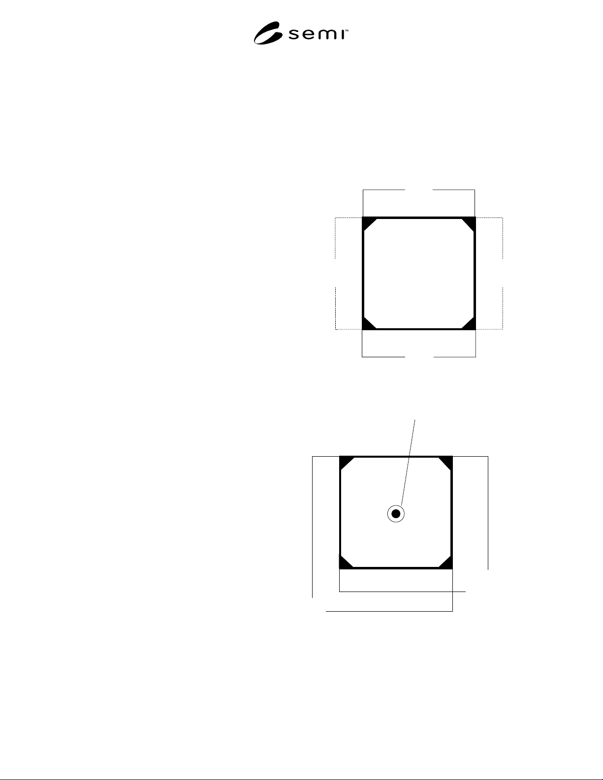
10.4 Resistivity Measurement (see Figure 1)
Measure the temperature, T
1
, of the specimen. Set the
current magnitude, I, to the desired value in a linear
region. Measure the voltages V
1
at I
1
and V
2
at I
2
. T
1
shall be 25 ± 5°C and the fluctuation of T
1
shall be
maintained to ± 1°C during the resistivity measurement.
10.5 Hall Mobility Measurement (see Figure 2)
10.5.1 Position the specimen between the magnet-pole
pieces so that the magnetic flux is perpendicular to the
two flat faces of the specimen.
10.5.2 Measure the temperature, T
2
, of the specimen.
Set the current magnitude, I, to the desired value.
Measure the voltage V
3
with the magnetic flux and V
4
without the magnetic flux.
10.5.3 T
2
shall be 25 ± 5°C and the fluctuation of T
2
shall be maintained to ± 1°C during Hall mobility
measurement.
SEMI M39-0999 © SEMI 19993
11 Calculations
11.1 Resistivity
ρ = (π × t/2 ln2) × (R
1
+ R
2
) × f(R
1
/R
2
) [Ω⋅cm]
where:
t is the specimen thickness,
R
1
and R
2
are the equivalent resistances
for two opposite sides as follows:
R
1
= V
1
/I
1
R
2
= V
2
/I
2
f(R
1
/R
2
) is the correction factor for specimen
shape.
In the case of R
1
/R
2
< 10,
f(R
1
/R
2
) = 1 − 0.34657A − 0.09236A
2
where: A = [(R
1
/R
2
− 1)/(R
1
/R
2
+ 1)]
2
11.2 Hall Mobility
µ = (t/B) × R
3
/ρ [cm
2
/ V⋅s]
where:
B is the magnetic flux density,
R
3
= V
3
-V
4
/ I
where:
V
3
is the voltage when the current is I under
magnetic flux
V
4
is the voltage when the current is I without
magnetic flux.
11.3 Temperature Conversion
11.3.1 Resistivity
ρ
T
= ρ
T1
⋅exp[−Ea/k⋅(1/T
1
− 1/T)]
where:
Ea is the activation energy (= 0.75eV)
k is the Boltzman constant (= 8.61E − 5 eV/K)
ρ
T
is the resistivity at T(K)
11.3.2 Hall Mobility
µ
T
= µ
T2
(T/T
2
)
−3/2
where: µ
T
is the Hall mobility at T(K)
12 Report
12.1 The following information shall be included in
the report for referee and research measurement:
12.1.1 Identification of test specimen,
12.1.2 Test temperature,
12.1.3 Specimen shape used, orientation, and corre-
sponding dimensions,
12.1.4 Magnitude of magnetic-flux density, and
12.1.5 Calculated resistivity and Hall mobility.
V
1
V
2
I
2
1
2
3
4
I
1
Figure 1
Block Diagram of Resistivity Measurement
V
3
or V
4
I
1
2
3
4
Magnetic field
Figure 2
Block Diagram of Hall Mobility Measurement