semi合集-English.pdf - 第4885页
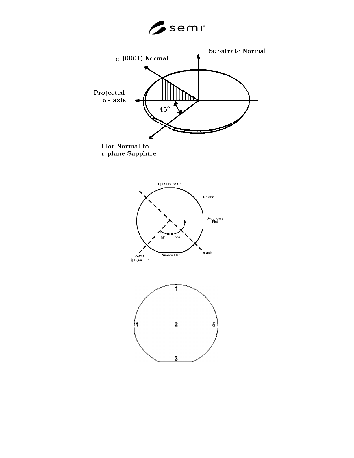
SEMI M3-0304 © SEMI 1978, 2004 5 Figure 2 Sapphire Surface Orientation Figure 3 Primary and Secondary Fl at Locations Figure 4 Measurement Points for Determination of Layer Thickness Variation
SEMI M3-0304 © SEMI 1978, 2004 4
meet the requirements, the material may be subject to
rejection.
13 Packing and Marking
13.1 Special packing requirements shall be subject to
agreement between the supplier and the purchaser.
Otherwise all slices shall be handled, inspected, and
packed in such a manner as to avoid chipping,
scratches, and contamination, and in accordance with
the best industry practices to provide ample protection
against damage during shipment.
13.2 The substrates supplied under these specifications
shall be identified by appropriately labeling the outside
of each box or other container, and each subdivision
thereof, in which it may reasonably be expected that the
substrates will be stored prior to further processing.
Identification shall include, as a minimum, the nominal
diameter, orientation, and lot number. The lot number,
either (1) assigned by the original manufacturer of the
substrates, or (2) assigned subsequent to substrate’s
manufacture, but providing reference to the original lot
number, shall provide ready access to information
concerning the fabrication history of the particular
substrates in that lot. Such information shall be
retained on file at the manufacturer’s facility for at least
one month after that particular lot has been accepted by
the purchaser.
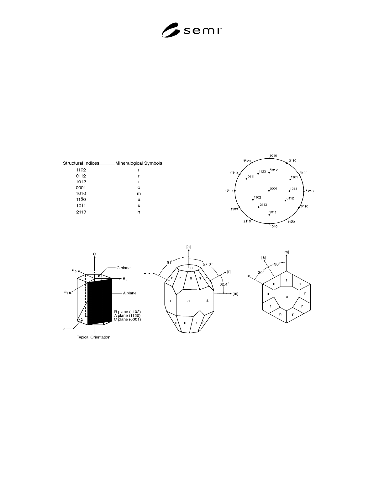
[n]
[m]
Figure 1
Sapphire Crystallographic Diagrams
SEMI M3-0304 © SEMI 1978, 2004 5
Figure 2
Sapphire Surface Orientation
Figure 3
Primary and Secondary Flat Locations
Figure 4
Measurement Points for Determination of Layer Thickness Variation
SEMI M3-0304 © SEMI 1978, 2004 6
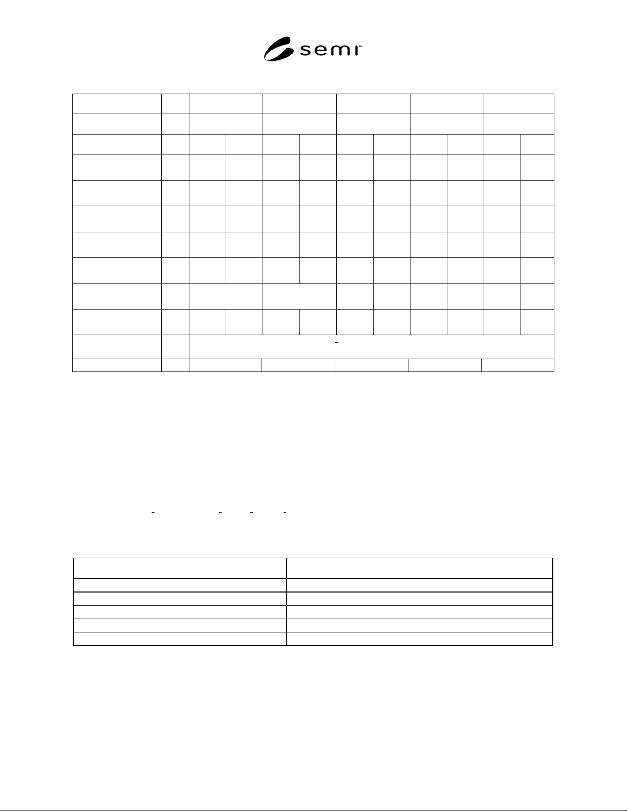
Table 1 Dimensional Specification for Sapphire Substrates
Nominal Diameter 2 inch 3 inch 100 mm 125 mm 150 mm
Previous Standard SEMI M3.2-91 SEMI M3.4-91 SEMI M3.5-92 SEMI M3.7-91 SEMI M3.8-91
Property Units Min Max Min Max Min Max Min Max Min Max
DIAMETER mm
in.
50.55
1.990
51.05
2.010
76.95
2.990
76.45
3.010
99.0
3.90
101.0
3.97
124.0 126.0 149.0 151.0
THICKNESS,
CENTER POINT
µ m
in.
280
0.011
380
0.015
380
0.15
480
0.19
500
0.0197
550
0.0216
600 650 650 700
PRIMARY FLAT
LENGTH
mm
in.
14.23
0.56
17.52
0.69
19
0.75
25
1.00
30.0
1.182
35.0
1.377
40.0 45.0 55.0 60.0
SECONDARY FLAT
LENGTH
mm.
in.
6.35
0.25
9.65
0.38
9.6
0.38
12.7
0.50
16.0
0.630
20
0.787
18.0 22.0 35.0 40.0
BOW, max µ m
in.
38
0.0015
51
0.002
40 60 60
WARP, max µ m
in.
Not Specified Not Specified
40 60 60
TOTAL THICKNESS
VARIATION, max
µ m
in.
51
0.002
76
0.0030
56
0.0019
50 60
SURFACE
ORIENTATION
}0211{
± 2.0° (NOTE 3)
NOTES 1 1 2 2 2
NOTE 1: For referee purposes, the U.S. Customary units apply. Conversion to metric (SI) equivalents was done following the maximum-
minimum convention in which the minimum values are rounded up and the maximum values are rounded down to ensure that the equivalent
range is always inside the referee range. If the metric equivalents are used for incoming inspection measurements, the rightmost digit of
minimum values should be reduced by 1 and the rightmost digit of maximum values should be increased by 1 to avoid rejection of material that is
within the specification when measured by the referee system of units. CAUTION — The significance of the rightmost digit may vary,
depending on the quantity being measured and the precision of the test procedure. Refer to the relevant test method for precision data that can be
used to construct appropriate guard bands.
NOTE 2: For referee purposes, the metric (SI) units apply. Conversion to U.S. Customary equivalents was done following the maximum-
minimum convention in which the minimum values are rounded up and the maximum values are rounded down to ensure that the equivalent
range is always inside the referee range. If the metric equivalents are used for incoming inspection measurements, the rightmost digit of
minimum values should be reduced by 1 and the rightmost digit of maximum values should be increased by 1 to avoid rejection of material that is
within the specification when measured by the referee system of units. CAUTION — The significance of the rightmost digit may vary,
depending on the quantity being measured and the precision of the test procedure. Refer to the relevant test method for precision data that can be
used to construct appropriate guard bands.
NOTE 3: Equivalent
}0211{ r planes are ),0121(and),2101(),0211( see Figure 1.
Table 2 Flatness Classes for Sapphire Substrates
Class Flatness (TIR), µm
I 25 max
II 14 max
III 10 max
IV 8 max
V 6 max