semi合集-English.pdf - 第6013页
SEMI G1-96 © SEMI 1 980, 199 6 6 Figure 5 9.4.5.2 L ead Misalignment to C eramic B a se — 0.0 10" (0.2 54 mm) ma ximu m (see Fig ure 6) . Figure 6 9.4.5.3 W indow Assembl y Mis alignme n t — 0.015" (0.358 mm ) …
SEMI G1-96 © SEMI 1980, 19965
9.4 Leadframe
NOTE 6: The criteria described in this section generally apply
to leadframe inspection for purchased sub-assemblies. Where
appropriate, the criteria may be used for sub-assemblies
manufactured in-house with purchased components. For
information on the criteria for leadframes purchased
separately, see SEMI G2.
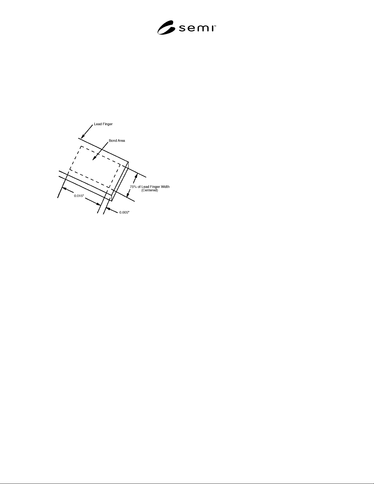
9.4.1 Lead Bond Areas — The minimum lead bond
area on the lead tip is defined in Figure 4.
Figure 4
9.4.1.1 Voids or Pits — Exposure of base metal with
any dimension greater than 0.001" (0.025 mm).
9.4.1.2 Discoloration, Blistering, or Peeling of the
Metallization
9.4.1.3 Scratches or Scrapes — Any b uild-up of
metallization or exposure of base metal.
9.4.1.4 Foreign Material, Including Glass Splatter or
Projections — No more than three sites, each with a
maximum dimension in any plane of 0.001" (0.025
mm).
9.4.1.5 Glass Wetting or Cracking — For purchased
sub-assemblies, any lead finger which is not firmly
embedded in the glass.
9.4.1.6 Glass Pullback from the Lead Tip — 0.010"
(0.254 mm) maximum.
9.4.1.7 Glass Bulge between Lead Fingers (Purchased
or In-House Sub-Assemblies) — 0.005" (0.127 mm)
height above the fingers except as agreed upon between
user and supplier for narrow pitch leads where this limit
may cause wire bond interference problems.
9.4.1.8 Lead Tip Coplanarity — 0.006" (0.15 mm)
maximum allowable difference in the position of the
top surface of the lead from highest lead to lowest lead.
9.4.1.9 Lead Tip Pitch — ± 0.002" (0.508 mm)
maximum allowable variation from true position.
9.4.2 Internal Lead Areas, Excluding Lead Bond
Areas
9.4.2.1 Burrs, Projections, and Pits — 0.002"
(0.508 mm) maximum allowable depth or height.
9.4.2.2 Foreign Material, Including Plating
Discoloration — 0.015" (0.381 mm) maximum surface
dimension or exceeding 0.002" (0.508 mm) in height.
9.4.2.3 Voids — Any exposure of base metal with a
major dimension greater than 0.002" (0.508 mm).
9.4.2.4 Blistering or Peeling of Metallization
9.4.2.5 Scratches and Scrapes — Any build-up of
metallization or exposure of base metal.
9.4.3 External Lead Areas — Unplated
NOTE 7: Non-functional areas of the leadframe, such as tie
bars, shall not be subjected to inspection unless they interfere
with handling equipment.
9.4.3.1 Scratches — Any scratch causing a loss of
more than 25% of the leadframe thickness.
9.4.3.2 Voids — Any void which violates the criteria
of Section 9.4.3.1 or causes a loss of more than 10% of
the design width of a leadframe detail.
9.4.3.3 Burrs — In excess of 0.002" (0.051 mm) in
height and 0.005" (0.127 mm) in the major dimension.
9.4.4 External Leads — Plated
NOTE 8: Non-functional areas of the leadframe, such as tie
bars, shall not be subjected to inspection unless they interfere
with handling equipment.
9.4.4.1 Scratches — Any scratch causing a loss of
more than 25% of the leadframe thickness.
9.4.4.2 Voids — Any void which violates the criteria
of Section 9.4.3.1 or causes a loss of more than 10% of
the design width of leadframe detail.
9.4.4.3 Burrs — In excess of 0.002" (0.051 mm) in
height and 0.005" (0.127 mm) in the major dimension.
9.4.4.4 Scratches and Scrapes — Any exposure of the
base metal or loss of plating integrity over more than
5% of a lead finger.
9.4.4.5 Voids — Any exposure of base metal.
9.4.4.6 Blistering or Peeling
9.4.5 Leadframe/Base/Window Assembly
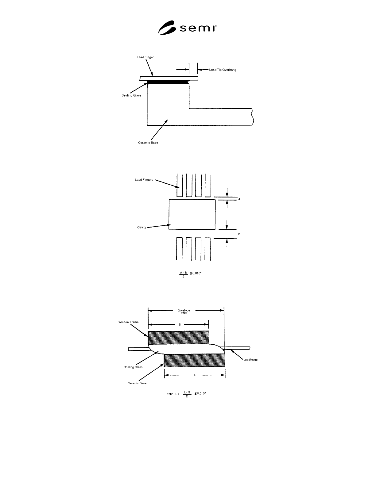
9.4.5.1 Lead Tip Overhang — 0.010" (0.254 mm)
maximum from the cavity wall (see Figure 5).
SEMI G1-96 © SEMI 1980, 1996 6
Figure 5
9.4.5.2 Lead Misalignment to Ceramic Base — 0.010" (0.254 mm) maximum (see Figure 6).
Figure 6
9.4.5.3 Window Assembly Misalignment — 0.015" (0.358 mm) maximum (see Figure 7).
Figure 7
9.4.6 Die-Attach Pad (Leadframe)
9.4.6.1 Flatness across the pad and parallelism to the base and window shall be agreed upon between user and
supplier.

SEMI G1-96 © SEMI 1980, 19967
9.4.6.2 Voids or Pits — Exposure of base metal with
any dimension greater than 0.001" (0.025 mm).
9.4.6.3 Discoloration, Blistering, or Peeling of the
Metallization
9.4.6.4 Scratches or Scrapes — Any b uild-up of
metallization or exposure of base metal.
9.4.6.5 Foreign Material, Including Glass Splatter or
Projections — No more than three sites, each with a
maximum dimension in any plane of 0.001" (0.025
mm).
9.4.7 Mechanical Damage — Leads
9.4.7.1 Broken, Kinked, or Missing Leads
9.4.7.2 Twist — Any lead twisted by more than 10°
from the untwisted condition.
9.4.7.3 Bottom-Formed Width — Any sub-assembly
with the bottom-formed width of the leadframe
exceeding ± 0.010" (0.254 mm).
9.4.7.4 Top-Formed Width — Any sub-assembly with
the top-formed width of the leadframe exceeding ±
0.010" (0.254 mm).
10 Incoming Inspection and Functional Tests
10.1 Incoming Inspection
10.1.1 Dimensional Inspection per Section 7.
10.1.2 Visual inspection per Section 9 at 10×
magnification with vertical lighting.
10.1.3 Metallization
10.1.3.1 Die-Attach Metallization — Thickness shall
be measured by standard cross-sectioning without
smearing or by X-ray fluorescence.
10.1.3.2 Lead Bond Metallization — Thickness shall
be measured by X-ray fluorescence.
10.1.3.3 External Lead Plating (If Applicable) —
Thickness shall be measured by X-ray fluorescence.
10.1.4 Lead Solderability (If Applicable) — Tested in
accordance with MIL-STD-883, Method 2003.
10.2 Functional Testing
NOTE 9: All procedures to functionally test the components
or sub-assemblies shall be agreed upon between user and
supplier.
The sequence of functional testing (and subsequent
environmental testing) shall be as shown in Figure 8.