semi合集-English.pdf - 第6210页
SEMI G42-0996 © SEMI 1986, 2004 13 Figure 11 Location of P ackage While Mounting on Test Board
SEMI G42-0996 © SEMI 1986, 2004 12
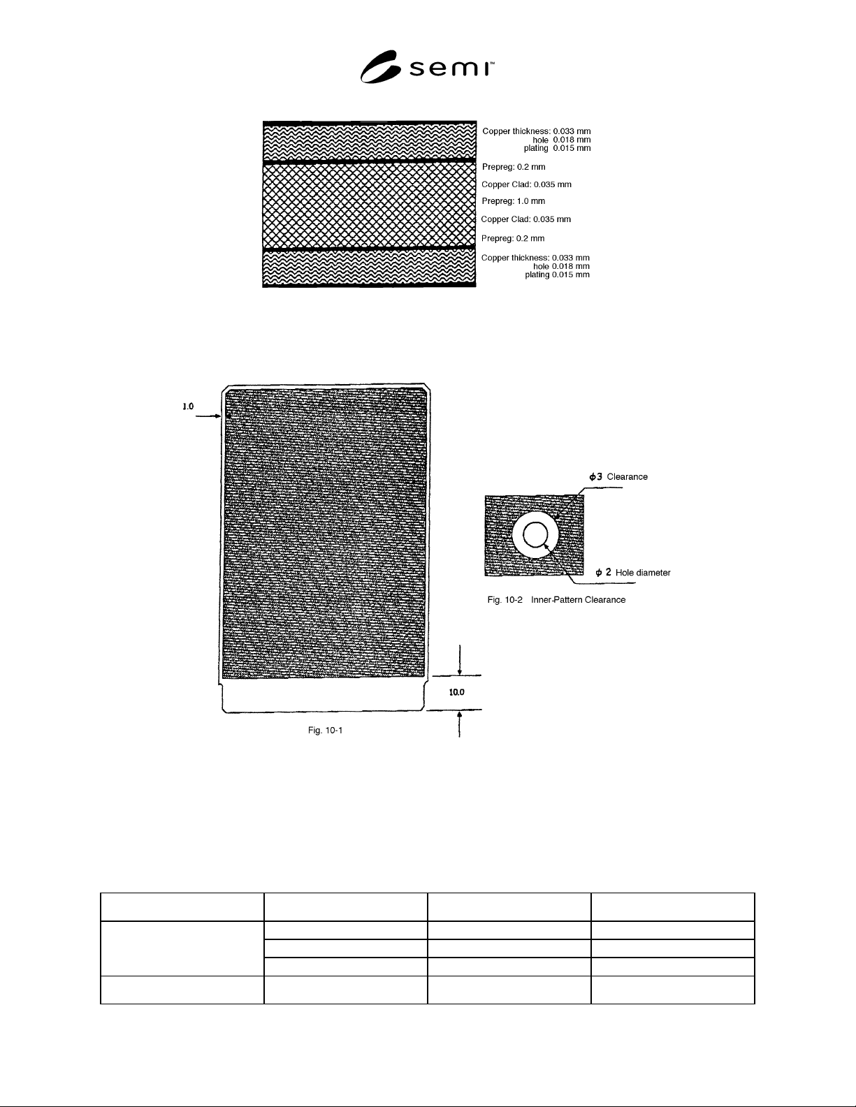
Figure 9
Multi-Layer Board Construction
Figure 10
Inner Layer Pattern and Clearance for Multi-Layer Thermal Test Board
1. Material: Epoxy Glass 1.0 mm Isolation thickness, FR-4 (Green)
2. Inner Copper Clad thickness: 0.035 µm
3. Tolerance: ± 0.1 mm (Unless noted)
Table 3 Clearance Diameter
Pitch (mm) Hole Diameter Ø 2 (mm) Clearance Diameter Ø 3 (mm)
1.5 0.4 1.2
1.27 0.35 1.1
BGA
1.0 0.3 0.9
PGA
2.54 0.95 1.7
SEMI G42-0996 © SEMI 1986, 2004 13
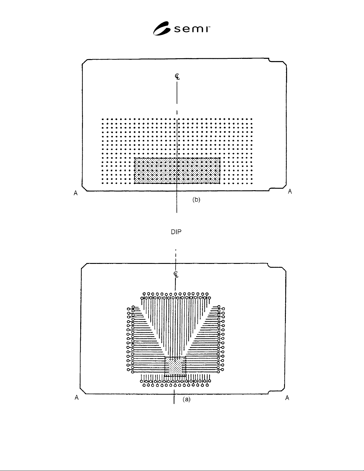
Figure 11
Location of Package While Mounting on Test Board
SEMI G42-0996 © SEMI 1986, 2004 14
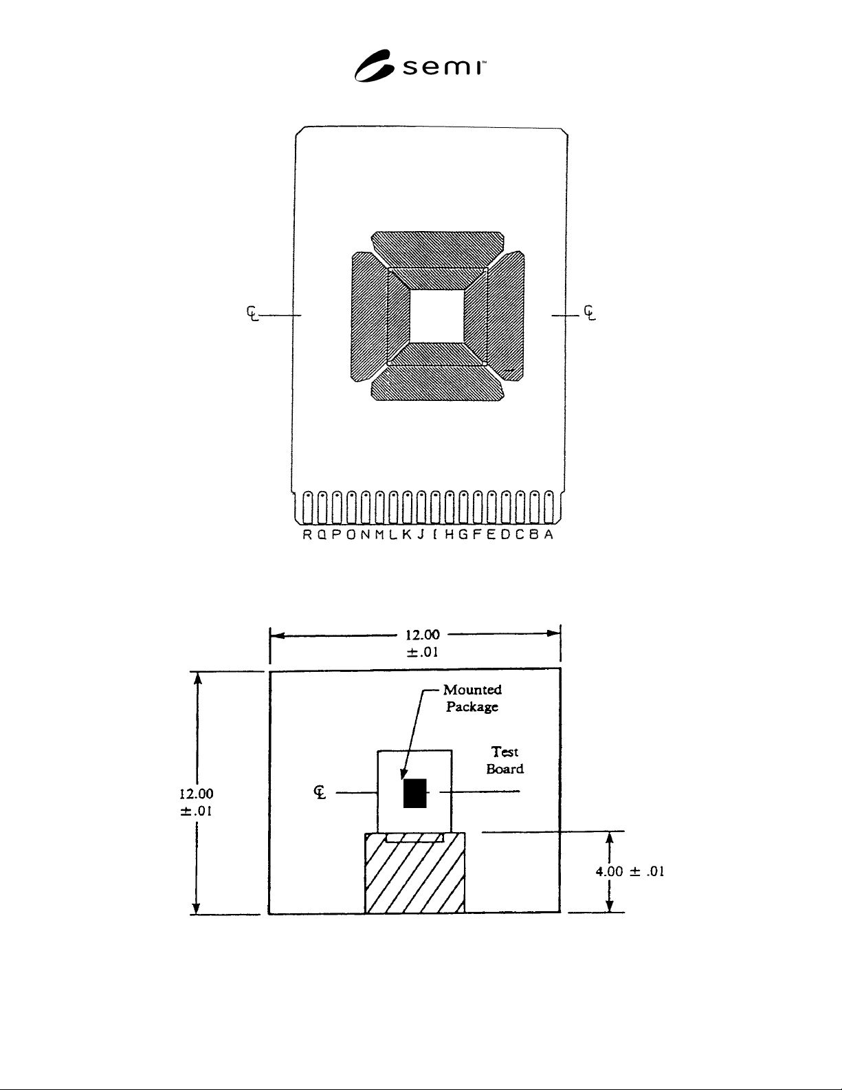
Figure 12
Location of Package While Mounting on Test Board (QFP)
Figure 13
Test Board Positioning Inside Measuring Chamber