semi合集-English.pdf - 第4194页
SEMI F72-1102 © SEMI 2002 5 APPENDIX 1 DISCUSSION OF EFFECTS OF DEPTH OF ANALYSIS ON DEPTH PROFILE ANALYSIS BY AUGER ELECTRON SPECTROSCOPY FOR SURFACE CHEMISTRY ANALYSIS OF PASSIVATED STAINLESS STEEL NOTE: The material i…
SEMI F72-1102 © SEMI 2002 4
spectral resolution and signal/noise, and that has at least
ten data points in each spectral window. The depth
profile should be continued into the depth of the sample
until the Fe, Cr and Ni levels are approximately
constant.
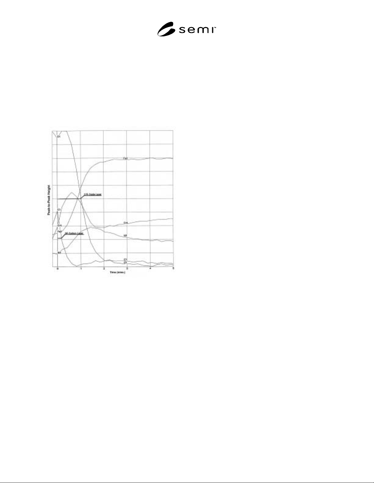
14.6 Depth profile data are presented as signal intensity
of each element with etch time (i.e., depth), and as
atomic concentration with etch time. Depths may be
estimated from etch times by determination of the etch
rate on a known thickness of standard material. A
typical AES profile is shown in Figure 2.
Figure 2
Auger Depth Profile of Stainless Steel
15 Calculations and Interpretation of Results
15.1 Most manufacturers supply software for
calculation of the approximate elemental composition
from the survey spectrum and the depth profile data.
The elemental composition should be estimated using
sensitivity factors appropriate to the instrument, each
element, and resolution settings for each measurement.
AES spectra are considered only semiquantitative, due
to instrument geometry and the chemical form
dependency of each element's sensitivity factor.
Evaluations of elemental composition should therefore
be limited to similar samples analyzed on the same
instrument.
15.2 The signal intensity with etch time graph may be
used to calculate oxide thickness, defined as the point at
which the oxygen signal decreases to half its maximum
value. The thickness of surface carbon contamination
is calculated in the same way from the carbon signal.
15.3 Relative abundances of profiled elements are
recorded on the atomic concentration with etch time
graph.
16 Reporting Results
16.1 A tabular summary of estimated surface elemental
composition is to be supplied with its associated
elemental survey spectrum.
16.2 Tabular summaries of oxide thickness, thickness
of the region in which Cr concentration exceeds Fe
concentration, thickness of a surface Fe enrichment (if
present), and carbon thickness are to be supplied with
associated depth profile graphs.
16.3 Optionally, parameters such as maximum Cr/Fe
ratio may be reported. However, the value of the
maximum Cr/Fe ratio is subject to instrument geometry
and sensitivity factor variations, and should not be used
for primary evaluation purposes. Comparative
evaluations should only be made from data collected by
the same instrument with an identical protocol.
16.4 Data acquisition parameters, including instrument
geometry, electron beam size or scan area, and other
pertinent settings are to be supplied. The manufacturer
and model number of instrument used is to be reported.
Analyst identity and analysis date are also required
information. Each table and graph must be clearly
labeled with sample identification.
NOTICE: SEMI makes no warranties or
representations as to the suitability of the standards set
forth herein for any particular application. The
determination of the suitability of the standard is solely
the responsibility of the user. Users are cautioned to
refer to manufacturer's instructions, product labels,
product data sheets, and other relevant literature,
respecting any materials or equipment mentioned
herein. These standards are subject to change without
notice.
By publication of this standard, Semiconductor
Equipment and Materials International (SEMI) takes no
position respecting the validity of any patent rights or
copyrights asserted in connection with any items
mentioned in this standard. Users of this standard are
expressly advised that determination of any such patent
rights or copyrights, and the risk of infringement of
such rights are entirely their own responsibility.
SEMI F72-1102 © SEMI 2002 5
APPENDIX 1
DISCUSSION OF EFFECTS OF DEPTH OF ANALYSIS ON DEPTH
PROFILE ANALYSIS BY AUGER ELECTRON SPECTROSCOPY FOR
SURFACE CHEMISTRY ANALYSIS OF PASSIVATED STAINLESS
STEEL
NOTE: The material in this appendix is an official part of SEMI F72 and was approved by full letter ballot procedures. This
appendix was derived from presentations made to the Stainless Steel and Surface Analysis Workshop
2
.
2 Stainless Steel and Surface Analysis Workshop, March, 1999; Interpratation of Depth Profile Analysis Data, Dave Harris, Charles Evans and
Associates.
A1-1
A1-1.1 The purpose of this appendix is to describe the
Auger Electron Spectroscopy (AES) technique and
explain the interpretation of the depth profile analysis
with respect to the structure and composition of the
passive oxide layer on stainless steel. The effect of the
depth of analysis on the measured chromium to iron
ratio, the oxide thickness, and the depth of enrichment
is discussed. The discussion also applies to depth
profile analyses performed by ESCA (Electron
Spectroscopy for Chemical Analysis, sometimes
referred to as X-Ray Photoelectron Spectroscopy, or
XPS).
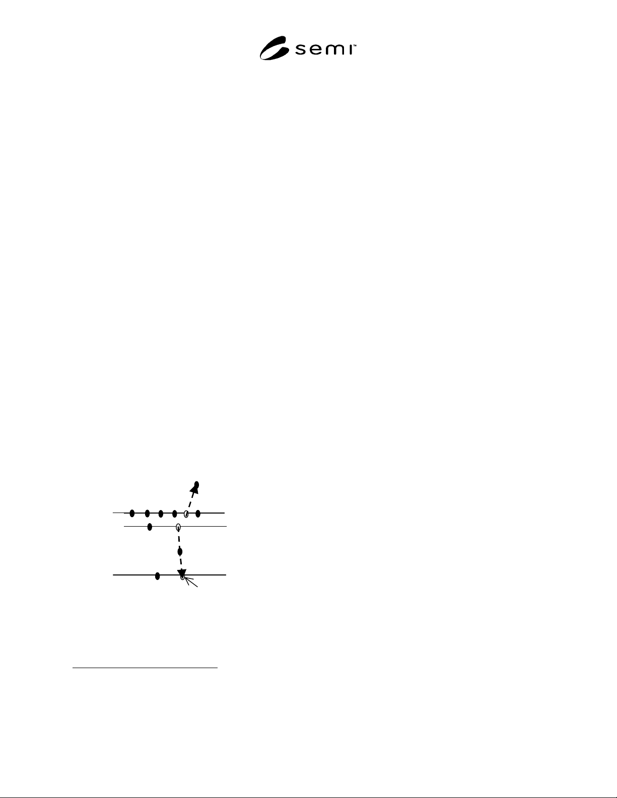
A1-1.2 Auger — The mechanism of Auger electron
generation is illustrated in Figure A1-1. The energy of
the Auger electron is determined by the energies of the
electron energy levels participating in the generation
process and are unique for each chemical element.
Thus the elements present in the analyzed region may
be determined by analysis of the energies of emitted
Auger electrons.
K or 1s
Auger Electron
L
2
,
3
or 2p
L
1
or 2s
Electron
Energy
Levels
Electron Hole
1
.
Electron from higher energy
level drops into electron hole
created by incident electron or
photon
2. Energy released by 1
“kicks out” Auger Electron
from hi
g
her ener
gy
level
Figure A1-1
Schematic Representation of Auger Electron
Generation Process
A1-1.3 The Auger technique makes use of an electron
beam for primary excitation, typically of energy in the
range 2 to 5 keV. The electron beam may by defocused
to analyze a relatively large area of the surface, of the
order of micrometers, or focussed and rastered to
“map” the distribution of elements on the surface. An
electron energy analyzer is focused at the same point as
the incident electron beam, and the Auger electrons that
escape the surface are detected and analyzed. The
analysis is commonly presented as the derivative of the
electron signal intensity N as a function of energy E,
dN(E)/dE, of the spectrum to enhance the visibility of
the small Auger electron peaks relative to the
background. An example of an Auger electron
spectroscopy spectrum of a stainless steel surface is
shown in Figure 1 of this test method.
A1-2 Illuminated Volume and Surface
Sensitivity
A1-2.1 The incident electron beam penetrates well
below the surface. Auger electrons are generated all
through this illuminated volume. The Inelastic Mean
Free Path (IMFP) of an electron in a solid is the mean
distance through the solid that an electron can travel
before losing some of its energy (suffering an inelastic
interaction). The IMFP is a function of the electron’s
energy and the matrix through which it is traveling.
Electrons with an energy typical of Auger and ESCA
electrons, approximately 1 keV, have an IMFP of about
10 angstroms. That means that a 1 keV electron will
travel, on average, 10 angstroms before interacting with
the matrix and giving up some of its energy. In other
words it will be scattered to lower energy and will not
be part of the photoelectron or Auger electron line for
its element. The IMFP is a statistical parameter and an
electron may travel several IMFPs before having a
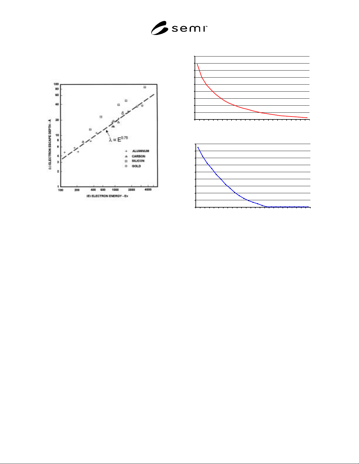
collision. The “several IMFPs” is called the escape
depth of the electron, or the depth of analysis, as shown
SEMI F72-1102 © SEMI 2002 6
in Figure A1-2. Although Auger and ESCA are
considered surface analytical tools, their depth of
analysis is on the order of 50 angstroms, or about one to
three times the depth of the oxide film found on a
typical passivated stainless steel surface.
Figure A1-2
The Electron Escape Depth of Low Energy
Electrons in Some Metals
A1-3 Depth of Analysis Function
A1-3.1 There has been some discussion with respect
to the “Depth of Analysis Function”. There is one
school that believes that it is 5 IMFPs and another that
uses 3 IMFPs. These two functions will be referred to
as 5λ and 3λ respectively. It will be seen that it makes
little difference which function is used even though the
depth of the oxide films is of the order of the functions.
These functions are seen in Figure A1-3, which shows
the proportion of the total signal generated from each
depth below the surface. The Y-axis is in decimal and
the X-axis is in angstroms from the surface. The first
point of the 5λ curve is 0.16 at the 1
st
angstrom level.
That means that 16% of the signal comes from the 1
st
angstrom, 14% from the 2
nd
angstrom level and so on
down to 1% from the 25
th
angstrom level. Thus
elements that do not appear on the surface or in the first
24 angstroms in from the surface, but do exist at the 25
angstrom level will be detected.
5 Lambda
0
0.02
0.04
0.06
0.08
0.1
0.12
0.14
0.16
0.18
1 2 3 4 5 6 7 8 9 10111213141516171819202122232425
Angstroms
3 Lambda
0
0.02
0.04
0.06
0.08
0.1
0.12
0.14
0.16
0.18
1 2 3 4 5 6 7 8 9 10111213141516171819202122232425
Angstroms
Figure A1-3
These Two Graphs Represent the “Depth of
Analysis” That Will be Seen When Analyzing 1 keV
Electrons. The Top Curve is the 5λ Curve and
Bottom the 3 λ.
A1-4 Modeling
A1-4.1 Figure A1-4 is the composition profile of a
“perfect” oxide. It represents 25 angstroms of pure
Cr
2
O
3
on an atomically flat 316L stainless steel surface,
with no surface or interfacial contamination present.
Figures A1-5a and b are the theoretical depth profiles
derived by assuming a depth of analysis of 5λ and 3λ
respectively. The first factor to note is that Fe, Ni and
Mo appear most or all of the way through the depth
profile of the oxide due to the contribution of the metal
substrate to the detected signal, the “depth of analysis”
effect as introduced above. 1 keV electrons can escape
from as deep as 25 angstroms. This must be
appreciated when interpreting these depth profiles.