semi合集-English.pdf - 第555页
SEMI E78-1102 © SEMI 1998, 2002 13 RELATED INFORMATION 1 STATIC CHARGE PROBLEMS NOTE: The ma terial contained in this re late d information is not an official part of SEMI E78 and is not intended to modify or supersede t…

SEMI E78-1102 © SEMI 1998, 2002 12
“X” indicates that the equipment passes ESD simulator testing at this
level.
NOTE 1: This level is subject to negotiation and has to be
specified in the dedicated equipment specification. If higher
voltages than those shown are specified, special test
equipment may be needed.
A1-2.3.2 Static Audit — While equipment may meet
the ESD immunity levels specified in IEC 6100-4-2, it
should be remembered that static charge levels in
manufacturing environments may be substantially
higher. Direct measurements of static charge are
difficult, and the presence of a charge does not always
imply that an ESD event causing an equipment
malfunction will occur. Some information may be
gained by using a fieldmeter to measure the
electrostatic field created by the surface charge.
Instruments known as EMI locators may also be used in
some cases to determine if ESD-related EMI is
occurring. Some representative measurements of
electric fields from objects in various areas of a
semiconductor wafer fab are as follows:
• Wet Etch — 0.1 kV/inch to 30 kV/inch
• Planarization — 0.1 kV/inch to 20 kV/inch
• Lithography — 0.1 kV/inch to 20 kV/inch
• Dry Etch — 0.1 kV/inch to 15 kV/inch
• Thin Film — 0.1 kV/inch to 15 kV/inch
• Diffusion — 0.1 kV/inch to 30 kV/inch
• Implant — 0.1 kV/inch to 15 kV/inch
A1-2.3.2.1 A knowledge of object capacitance and
other physical properties is needed to determine if any
of the above measurements indicate an equipment
hazard due to ESD events. However, the range of the
measurements strongly indicate that such ESD events
can occur. The examples in Related Information R1-3.3
support this conclusion.
A1-2.3.3 Guide Recommendations — Based on the
static audits and equipment test data, there appears to be
a wide range of static immunity in equipment as well as
in the static charge levels in work environments. As
stated previously, it is difficult to establish a direct
correlation between ESD events and fieldmeter
measurements made on products, carriers, or any other
objects in the work environment. The following
sensitivity levels are defined with recommended test
levels for each.
A1-2.3.3.1 Level 4 — Field measurements of static
charge at input/exit ports are expected to exceed 10
kV/inch. Equipment should pass ESD simulator testing
at 8 kV direct contact discharge, 18 kV air discharge.
Guide recommendation (Section 12.5) - 1200
nanocoulombs (8 kV × 150 picofarads).
A1-2.3.3.2 Level 3 — Field measurements of static
charge at input/exit ports are expected to exceed 4
kV/inch, but are less than 10 kV/inch. Equipment
should pass ESD simulator testing at 4 kV direct
contact discharge, 8 kV air discharge. Guide
recommendation (Section 12.5) - 600 nanocoulombs (4
kV × 150 picofarads).
A1-2.3.3.3 Level 2 — Field measurements of static
charge at input/exit ports are expected to exceed 500
V/inch, but are less than 4 kV/inch. Equipment should
pass ESD simulator testing at 2 kV direct contact
discharge, 4 kV air discharge. Guide recommendation
(Section 12.5) - 300 nanocoulombs (2 kV × 150
picofarads).
A1-2.3.3.4 Level 1 — Field measurements of static
charge at input/exit ports are expected to exceed zero,
but are less than 500 V/inch. Equipment should pass
ESD simulator testing at 1 kV direct contact, 2 kV air
discharge. Guide recommendation (Section 12.5) - 150
nanocoulombs (1 kV × 150 picofarads).
NOTICE: SEMI makes no warranties or
representations as to the suitability of the standards set
forth herein for any particular application. The
determination of the suitability of the standard is solely
the responsibility of the user. Users are cautioned to
refer to manufacturer’s instructions, product labels,
product data sheets, and other relevant literature
respecting any materials mentioned herein. These
standards are subject to change without notice.
The user’s attention is called to the possibility that
compliance with this standard may require use of
copyrighted material or of an invention covered by
patent rights. By publication of this standard, SEMI
takes no position respecting the validity of any patent
rights or copyrights asserted in connection with any
item mentioned in this standard. Users of this standard
are expressly advised that determination of any such
patent rights or copyrights, and the risk of infringement
of such rights, are entirely their own responsibility.

SEMI E78-1102 © SEMI 1998, 2002 13
RELATED INFORMATION 1
STATIC CHARGE PROBLEMS
NOTE: The material contained in this related information is not an official part of SEMI E78 and is not intended to modify or
supersede the guide in any way. These notes are provided as a source of information to aid in the application of the guide, and are
to be considered reference material. Determination of the suitability of the material is solely the responsibility of the user.
R1-1 ESD Damage
Contributed by Leo G. Henry, Ph.D., Advanced Micro
Devices, EOS/ESD/LU/EMC Department, Sunnyvale,
CA 94538, leogesd@pacbell.net.
R1-1.1 Introduction — ESD damage to devices occurs
when they come into contact with personnel and
equipment. Either may store a residual charge large
enough to destroy the device if a discharge occurs. In
the semiconductor industry, it has been established that
a significant proportion of customer field returns are
attributed to damage resulting from ESD.
R1-1.2 Description of ESD Damage Mechanisms —
ESD failures are the result of either a current-induced
phenomenon or a charge-induced phenomenon, and the
damage can either be junction, contact, dielectric or
oxide related. The apparent similarity in current-
induced damage resulting from ESD due to human
body model discharges (HBM) or machine model
discharges (MM) results from the thermal nature of
both of these process. The HBM and MM damages
result when the temperature (joule heating) of the
region dissipating the ESD pulse energy reaches a
critical value and melting occurs.
R1-1.2.1 Charge-induced phenomena are predicted by
the charged device model (CDM). For CDM type
discharges, oxide punch through occurs when the ESD
voltage applied across the oxide creates a high enough
field to break down the oxide. Excessive current flow
results, causing an oxide short, but there is no heat
transfer (adiabatic process).
R1-1.2.2 It should be noted here that the time duration
for typical ESD events from charged objects and
personnel ranges from 10 to 100 nanoseconds, while
CDM type events occur in less than 1 nanosecond.
R1-1.3 Device Testing Models
R1-1.3.1 Human Body Model (HBM) — The Human
Body Model is the oldest and the most widely used of
the three ESD models. The model attempts to replicate
the discharge from a real human when the latter touches
a device that is at a lower potential. The human
capacitance and resistance have been ideally chosen to
be 100 picofarads and 1500 ohms respectively. The
values were chosen after measurements were made on
humans in varying positions with respect to their
surroundings. The resulting discharge waveform has a
double exponential shape with risetime range of 2–10
nsec and a decay constant (1/e position) of 150 ± 20
nsecs. The typical peak currents range from 0.67 Amps
at 1000 volts to 2.67 Amps at 4000 volts.
R1-1.3.2 Machine Model (MM) — The Machine
Model is described by Electronic Industries Association
of Japan (EIAJ) as a worst case HBM. The model
attempts to replicate the discharge from a metallic arm
of an automatic handler coming into contact with the
metallic leads of a semiconductor device which is at a
lower potential. A capacitance of 200 picofarads and
ideally zero resistance produces a sinusoidal decaying
waveform with an effective pulse duration of 200 nsec.
The typical peak currents range from 1.75 Amps at 100
volts to 14.0 Amps at 800 volts. Note that MM failures
occur at 5–10 times lower voltage than HBM.
R1-1.3.3 Charged Device Model (CDM) — The
Charged Device Model in its purest form is actually a
field induced model because the device is actually part
of model. This model attempts to describe a device
which itself becomes charged due to an external field,
or due to triboelectric charging of the device surfaces.
During discharge, the parasitics (capacitance,
inductance and impedance) in the device play a
significant role in the resulting failure. The discharge
pulse is a sinusoidal waveform with an extremely fast
risetime of less than 500 picoseconds. The waveform
decays rapidly with a total pulse duration of less than 5
nano-seconds. The peak currents range from 2.0 Amps
at 250 volts charging voltage, to 18.0 Amps at 2000
volts charging voltage.
R1-1.3.4 Correlation Between Models — There is
much debate on whether or not there is any type of
correlation between HBM and MM. While some
companies report a correlation of roughly 10:1 between
the two models, other companies have seen anywhere
from 5–20:1 differences in passing voltages between
the two models. There is also no established voltage
correlation between CDM damage and HBM or MM
ESD events. In equipment, ESD damage events will be
related to the MM or CDM types of ESD. Users will
need to determine the type of ESD hazard to their
devices and choose the test method accordingly.
R1-1.4 ESD Laboratory Simulation Testing
R1-1.4.1 Description of Test Methods — Test
procedures discussed here for ESD simulation conform
SEMI E78-1102 © SEMI 1998, 2002 14
to those established by the ESD Association Standards
ESD STM 5.1 (for HBM), ESD S5.2 (for MM), and
MIL-STD-883, C/3015.7-method 8. The ESD
Association is presently considering two documents
related to CDM Testing. Details are to be found in these
standards.
R1-1.4.1.1 Devices are qualified at a level
corresponding to the highest ESD stress they are able to
withstand. These levels are discussed in more detail in
Appendix A1-2.1.
R1-1.4.2 Simulation Test Results — In general all units
must be data-logged both pre- and post-stress test. Any
leakage current equal to or greater than a specific
amount (company dependent — typically 10 micro-
amps or less) is “flagged” as a failure, and any current
shift greater than about 200 nano-Amp is marked on the
record.
R1-1.4.3 HBM Stress Testing — An R-C network is
used to simulate the ESD event. In an HBM ESD
Simulator, a high voltage is used to charge the capacitor
(100 pF) which discharges through the resistor (1500
ohms) into the device under test. The present draft
standard (1997) requires a minimum of two discharges
(1 positive and 1 negative) per voltage level.
R1-1.4.4 MM Stress Testing — An R-C network is also
used in the MM ESD Simulator for ESD testing. High
voltage charges the capacitor (200 pF) which
discharges through the short wire (zero ohm) into the
device under test. The present standard requires a
minimum of six discharges (3 positive and 3 negative).
R1-1.4.5 CDM Stress Testing — The package and
leadframe of the device are charged by direct charging
or field induction. For the Direct Charging Method,
direct contact is made to one of the device leads
connected to the substrate or bulk material of the
device. The device is then discharged via a one ohm
resistor to ground.
R1-1.4.5.1 For the Field Induced Method, the device is
placed on a metallic charging plate with the device
packaging material touching the plate. The potential of
the device is raised by applying a voltage to the
charging plate. The induced voltage on the device is
discharged to ground through a 1 ohm resistor that
contacts each device lead. The present draft standard
(1996) requires a minimum of 6 discharges (3 positive
and 3 negative) from each device lead.
R1-1.5 Examples of Damage from Device Testing
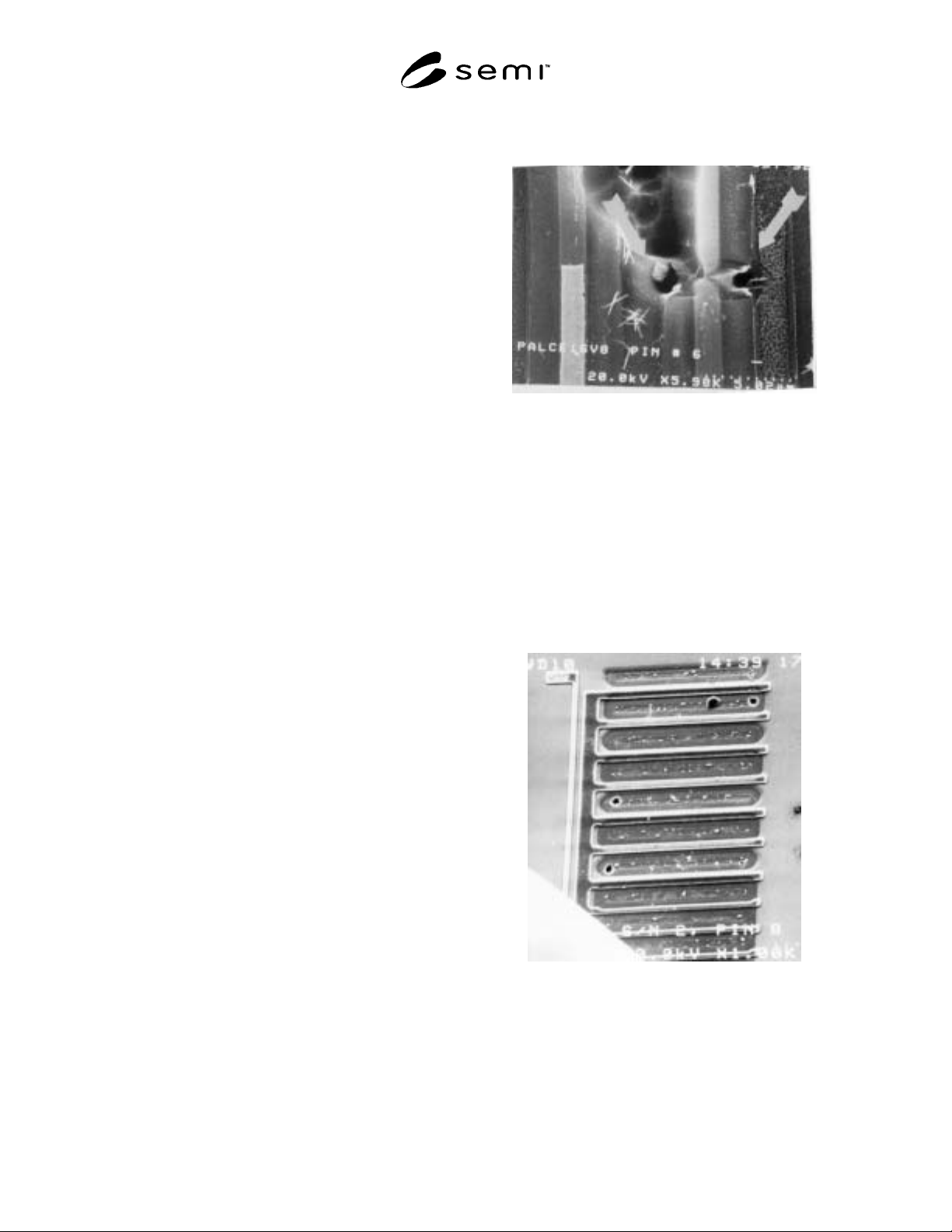
R1-1.5.1 HBM ESD Damage
Figure R1-1
Example of HBM Damage
R1-1.5.1.1 In this example of HBM damage (refer to
Figure R1-1), de-processing (removal of the processed
layers) down to the poly level and very high
magnification (SEM) examination were required in
order to see the failure site morphology of arcing from
source to drain within the ESD protective structures.
The electrical characteristics found were: resistive
shorts, leakages, low breakdown voltages and Icc
failures.
R1-1.5.2 MM ESD Damage
Figure R1-2
Example of MM Damage
R1-1.5.2.1 In the above MM example (refer to Figure
R1-2), the damage was more severe than for HBM. De-
processing down to the poly level and the SEM
examination showed the failure site morphology of
large deep pits occurring at the contact(s) suggesting