semi合集-English.pdf - 第994页
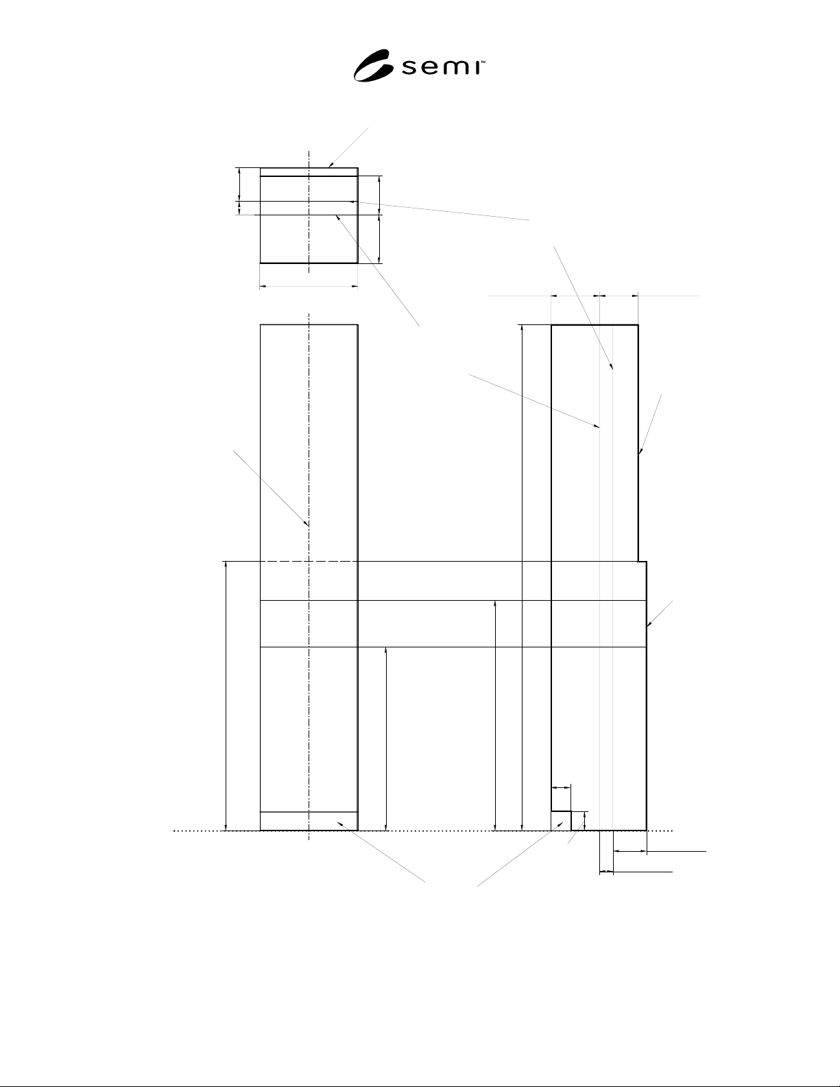
SEMI E131-0304 © SEMI 2004 4 plane Equipment Side View Front View L (E64) Top View bilateral datu m floor (E63) (when carrier is undocked) facial datum plane (E63) and removal) substrate insertion (when carrier is docked…
SEMI E131-0304 © SEMI 2004 3
be followed depending on the nominal wafer-seating
plane selected.
6.4 Maximum Outer Dimensions — If the IMM is
intended to be located at the front side of a tool (where
load ports are usually located), the outer dimensions of
the IMM shall not exceed the volume as it would be
used, when a load port is attached to a BOLTS-M
interface.
6.4.1 Depth — The depth of the IMM located at the
front of the process tool shall not exceed the maximum
depth of a load port. The entire depth of the IMM shall
not exceed the sum of y70 + y76 + D (from SEMI E63
and SEMI E15.1 respectively), as measured from the
BOLTS plane.
6.4.1.1 The IMM shall not extend toward the tool
beyond the BOLTS plane, except for possible
temporary use of the reserved space defined in SEMI
E63.
6.4.2 Width — If locating the IMM adjacent to another
load port, there are width requirements defined by the
carrier centroid spacing dimension S from SEMI E15.1.
6.4.2.1 If locating the IMM adjacent to an occupied
load port containing a FOUP with handles, then the
design of the width should not compromise the C1
clearance dimension from SEMI E15.1.
NOTE 3: Most tools today are designed with the dimension
S chosen for spacing of boxes with handles. If the IMM
width exceeds twice the x50 dimension for a FOUP with
handles (from SEMI E47.1) then the IMM may not comply
with the C1 requirement for integration with most existing
tools.
6.4.3 Height — A height H2 (from SEMI E15.1) is the
upper maximum boundary for the IMM when located at
the front of the tool.
6.4.4 Exclusion Volume — There is an exclusion
volume, defined by dimensions L
d
and L
h
at the bottom
rear of the IMM reserved for requirements from SEMI
E64. The width of this exclusion volume is the full
width of the tool.
6.4.5 The front of the IMM (towards the tool) between
the floor and up to the height of a load port, as given by
the sum of H (SEMI E15.1) plus z79 (SEMI E63), is
identical with the BOLTS plane. Above this height, the
front of the IMM is limited by the equipment boundary
as defined in SEMI E15.1.
NOTE 4: The BOLTS plane and the equipment boundary are
defined by a different set of dimensions and thus are at
different positions. The BOLTS plane is located more
towards the tool.
7 Related Documents
7.1 SEMI Standards
SEMI E6 — Guide for Semiconductor Equipment
Installation Documentation
SEMI E51 — Guide for Typical Facilities Services and
Termination Matrix
SEMI E62 — Specification for 300 mm Front-Opening
Interface Mechanical Standard (FIMS)
SEMI E101 — Provisional Guide for EFEM Functional
Structure Model
SEMI E106 — Provisional Overview Guide to SEMI
Standards for Physical Interfaces and Carriers for 300
mm Wafers
SEMI E131-0304 © SEMI 2004 4
plane
Equipment
Side ViewFront View
L (E64)
Top View
bilateral datum
floor
(E63)
(when carrier is undocked)
facial datum plane
(E63)
and removal)
substrate insertion
(when carrier is docked;
facial datum plane
BOLTS plane
(E63)
C
L
C
L
L
C
(E64)
Exclusion volume
(E64)
h
L
d
(E15.1)
boundary
(E63)
BOLTS plane
H2 (E15.1)
wafer-seating plane:
nominal
upper limit for
wafer-seating plane:
nominal
lower limit for
+(25-1)*z12 (E1.9)
+z8 (E1.9)
+z44 (E47.1)
H (E15.1)
+z8 (E1.9)
+z44 (E47.1)
H (E15.1)
+z79 (E63)
H (E15.1)
D (E15.1)
D1 (E15.1)
y76 (E63)
y70 (E63)
y70 (E63)
y76 (E63)
S (E15.1)
D (E15.1) D1 (E15.1)
Figure 1
IMM Dimensional Requirements
SEMI E131-0304 © SEMI 2004 5
RELATED INFORMATION 1
CALCULATION OF NOMINAL WAFER-SEATING PLANE
NOTICE: This related information is not an official part of SEMI E131 and was derived from work by the
originating task force. This related information was approved for publication by full letter ballot procedures on
December 4, 2003.
R1-1 The nominal wafer-seating plane is
calculated using values found in a number of
other standards, as follows.
R1-1.1 In SEMI E1.9 (the specification where this
plane is defined), the nominal wafer-seating plane is
referenced from the horizontal datum plane. SEMI
E15.1 defines the horizontal datum plane H to identify a
reference plane for positioning kinematic couplings.
While there are no kinematic couplings required for the
IMM, we use this same dimension as a starting point
for defining the nominal wafer-seating plane for wafer
insertion and removal. As in SEMI E15.1, the
horizontal datum plane is given at a height H relative to
the floor.
R1-1.2 Next, from SEMI E47.1 there is defined an
external horizontal datum plane (equal to the horizontal
datum plane from SEMI E15.1) and an internal
horizontal datum plane, where the internal horizontal
datum plane is located at a height of z44 above the
external horizontal datum plane.
R1-1.3 Then, FOUP slot number 1 is defined at a
height z8 in SEMI E1.9, but should be measured from
the internal horizontal datum plane from SEMI E47.1.
R1-1.4 Finally, z12 in SEMI E1.9 is the slot-to-slot
spacing within a cassette. So for a 25 substrate cassette,
the distance from the FOUP slot number 1 to slot 25 is
(25-1) * z12.
NOTICE: SEMI makes no warranties or
representations as to the suitability of the standards set
forth herein for any particular application. The
determination of the suitability of the standard is solely
the responsibility of the user. Users are cautioned to
refer to manufacturer' s instructions, product labels,
product data sheets, and other relevant literature,
respecting any materials or equipment mentioned
herein. These standards are subject to change without
notice.
By publication of this standard, Semiconductor
Equipment and Materials International (SEMI) takes no
position respecting the validity of any patent rights or
copyrights asserted in connection with any items
mentioned in this standard. Users of this standard are
expressly advised that determination of any such patent
rights or copyrights, and the risk of infringement of
such rights are entirely their own responsibility.
Copyright by SEMI® (Semiconductor Equipment and Materials
International), 3081 Zanker Road, San Jose, CA 95134. Reproduction o
f
the contents in whole or in part is forbidden without express written
consent of SEMI.