semi合集-English.pdf - 第6373页
NOTICE: SEMI makes no warranties or representations as to the suitability o f the standard set forth herei n for any pa rticular application. The determination of the suitability o f the standard is solely the responsibi…
11 Label Material and Adhesive
11.1 Label material should not generate particles.
11.2 Label adhesive should not prohibit recyclability of the shipping packages.
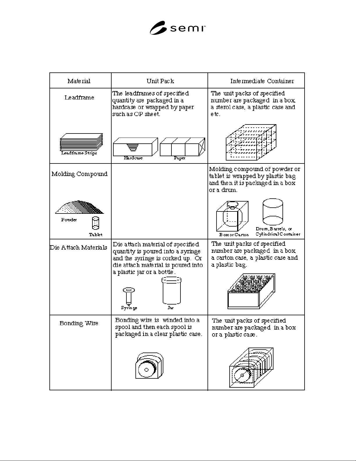
Figure 4
Definition of Packaging Forms for Leadframe, Molding Compound, Die Attach Material, and Bonding Wire
5 SEMI G71-0996 © SEMI 1996, 2004

NOTICE: SEMI makes no warranties or
representations as to the suitability of the standard set
forth herein for any particular application. The
determination of the suitability of the standard is solely
the responsibility of the user. Users are cautioned to
refer to manufacturer’s instructions, product labels,
product data sheets, and other relevant literature
respecting any materials or equipment mentioned
herein. These standards are subject to change without
notice.
By publication of this standard, SEMI takes no position
respecting the validity of any patent rights or copyrights
asserted in connection with any item mentioned in this
standard. Users of this standard are expressly advised
that determination of any such patent rights or
copyrights, and the risk of infringement of such rights,
are entirely their own responsibility.
SEMI G71-0996 © SEMI 1996, 2004 6
Copyright by SEMI® (Semiconductor Equipment and Materials
International), 3081 Zanker Road, San Jose, CA 95134. Reproduction of
the contents in whole or in part is forbidden without express written
consent of SEMI.

SEMI G72-0997 © SEMI 19971
SEMI G72-0997
SPECIFICATION FOR BALL GRID ARRAY DESIGN LIBRARY
1 Purpose
The purpose of this specification is to promote industry
use of common BGA designs that may be distinguished
by their form, fit, function, and reliability requirements
and to record designs by category that meet these
requirements.
2 Scope
2.1 This document provides a library of company-
sponsored BGA designs for the purpose of promoting
the use of these common designs and to minimize the
unnecessary proliferation of new designs. New designs
will be added as they become sponsored by and
approved by member companies.
2.2 This library shall include ceramic, plastic, tape,
metal and other (as new categories of designs are
identified and added to this specification) BGA designs
that are fully compliant with existing JEDEC-registered
or standard mechanical outlines. Proposals for new
designs may be balloted in parallel with congruent
JEDEC registrations or standards, but will not be
published in this library until such registration and/or
standard is an approved JEDEC outline.
2.3 Controlling dimensions are metric (Systems
International units).
3 Referenced Documents
3.1 SEMI Documents
SEMI International Standards Compilation of Terms
Regulations Governing SEMI Standards Committees
3.2 ASME
1
ASME Y14.5M-94 — Dimensioning and Tolerancing
3.3 EIA/JEDEC
2
EIA JEDEC Publication 95 — Registered and Standard
Outlines for Semiconductor Devices
JEDEC BGA Design Guide 95-1 — Section 14
J-STD-020 —
1 American Society of Mechanical Engineers, 22 Law Drive,
P.O. Box 2900, Fairfield, New Jersey 07007-2900.
2 Electronic Industries Association, Joint Electron Device
Engineering Council, 2500 Wilson Blvd., Arlington, VA 22201,
(703) 907-7560.
JESD 22-A113 — Preconditioning of Plastic Surface
Mount Devices Prior to Reliability Testing
4 Terminology
4.1 ball grid array (BGA) package — A square or
rectangular substrate package with an array of metallic
balls on one surface of the package. The metallic balls
form the electrical and mechanical connection between
the package and the PC board or socket.
4.2 column grid array — Same as ball grid array
except that metallic columns are used in place of the
metallic balls for the electrical and mechanical
interconnection between the package and the PC board.
NOTE 1: In the text of this specification, whenever ball grids
are mentioned, a reference to column grids is also implied.
4.3 wire bond ring — Metalized area in the shape of a
complete or partial ring surrounding the die mounting
area intended for group electrical interconnections.
5 Ordering Information
5.1 Order of Precedence — To avoid conflicts, the
order of precedence when ordering ball grid array
substrates or assembled packages when using BGA
Library Designs from this specification shall be as
follows:
a. Purchase Order
b. Customer BGA Drawing
c. BGA Library Design from this specification
d. Referenced Documents from Section 3.0
e. Other related documents
6 General Design Character istics Listing
Format
6.1 Each design addition to this library shall include a
general design characteristics description which shall be
listed in Appendix 1 of this specification and also be
formatted on top of the title block for each design
drawing.
6.1.1 Description listings in the General Design
Characteristics, Appendix 1 shall be organized into
category sections: Plastic, Ceramic, Tape, Metal, or
Other.
6.1.2 These descriptions shall be listed across a row of
characteristics classification columns and may
determine the uniqueness of each design.