semi合集-English.pdf - 第2638页
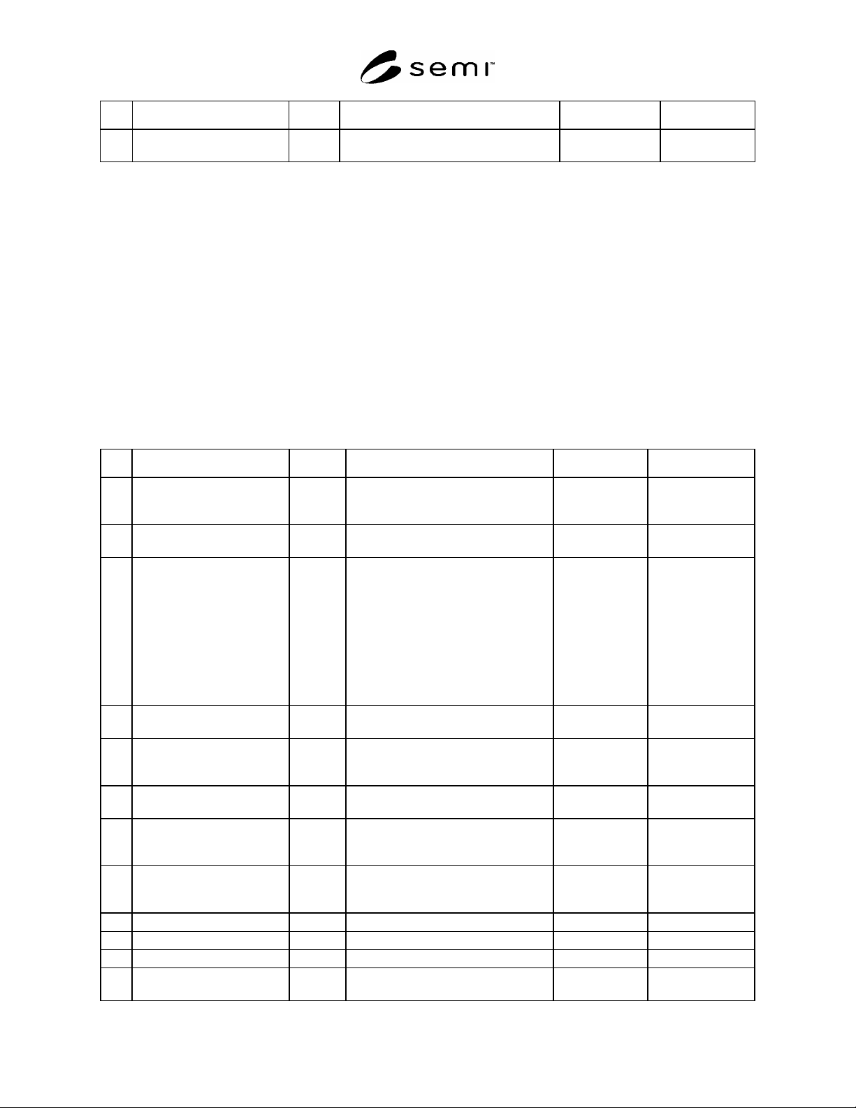
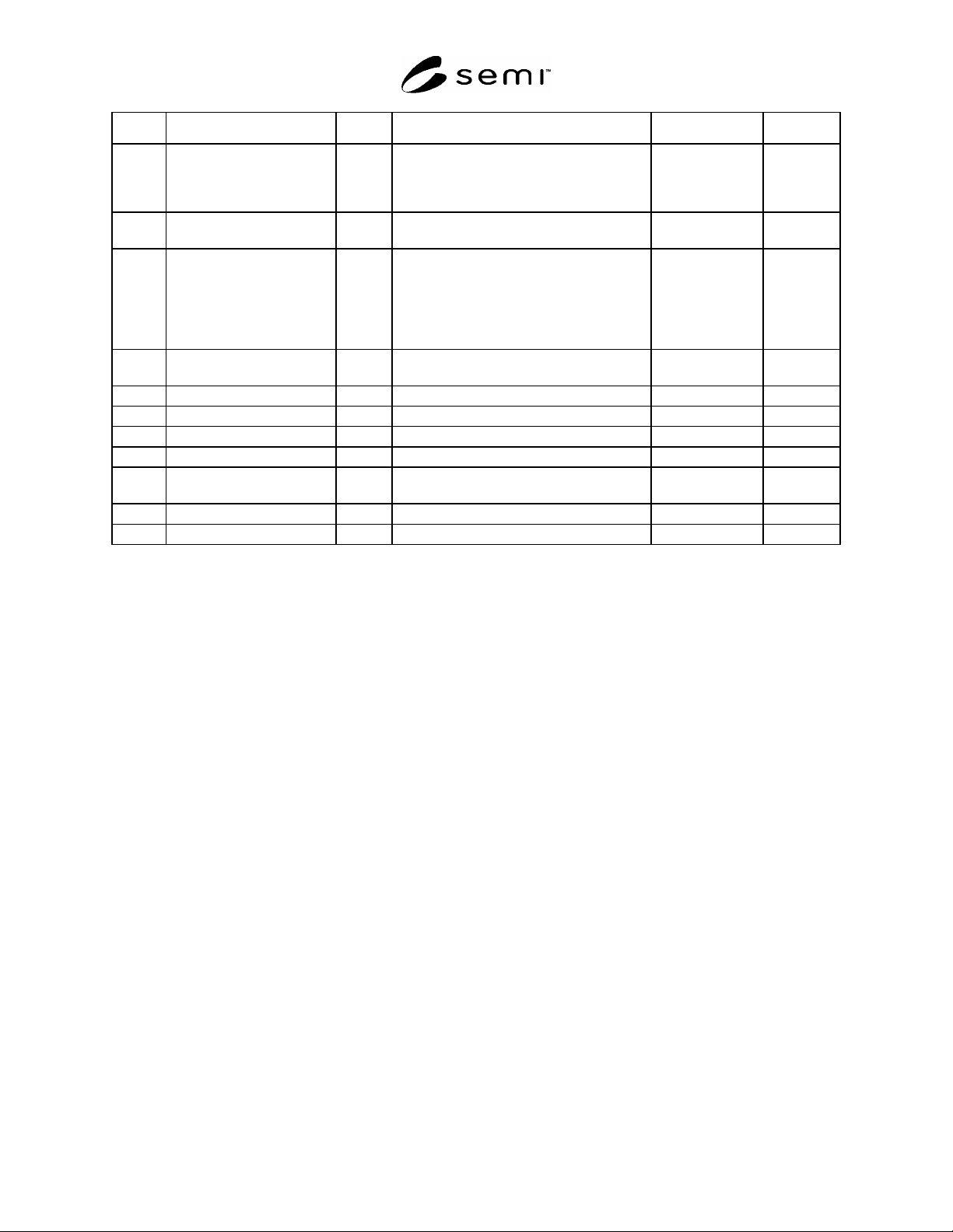
SEMI E94-0705 © SEMI 2000, 2005 21 # Comment Dir Message CJS PJS 12 Material processing starts after all materia l is in the processing boat. H<-E Event (PRJOBP ROCESSING, prj01_01) ACTIVE/ PROCESSING 13 Output carrie…
SEMI E94-0705 © SEMI 2000, 2005 20
# Comment Dir Message CJS PJS
15 Jobs may complete before the
carrier is picked up.
H<-E Event (ControlJobCompleted=cjf01_01,
status=OK)
COMPLETE
R1-2 ControlJob for a Single Wafer Processing Tool
R1-2.1 Will be added later.
R1-3 ControlJob for Single Wafer Processing with Recipe Variable Parameters
R1-3.1 Will be added later.
R1-4 Error Recovery of Batch Tool ControlJob, Carrier Slot Map Failure
R1-4.1 Will be added later.
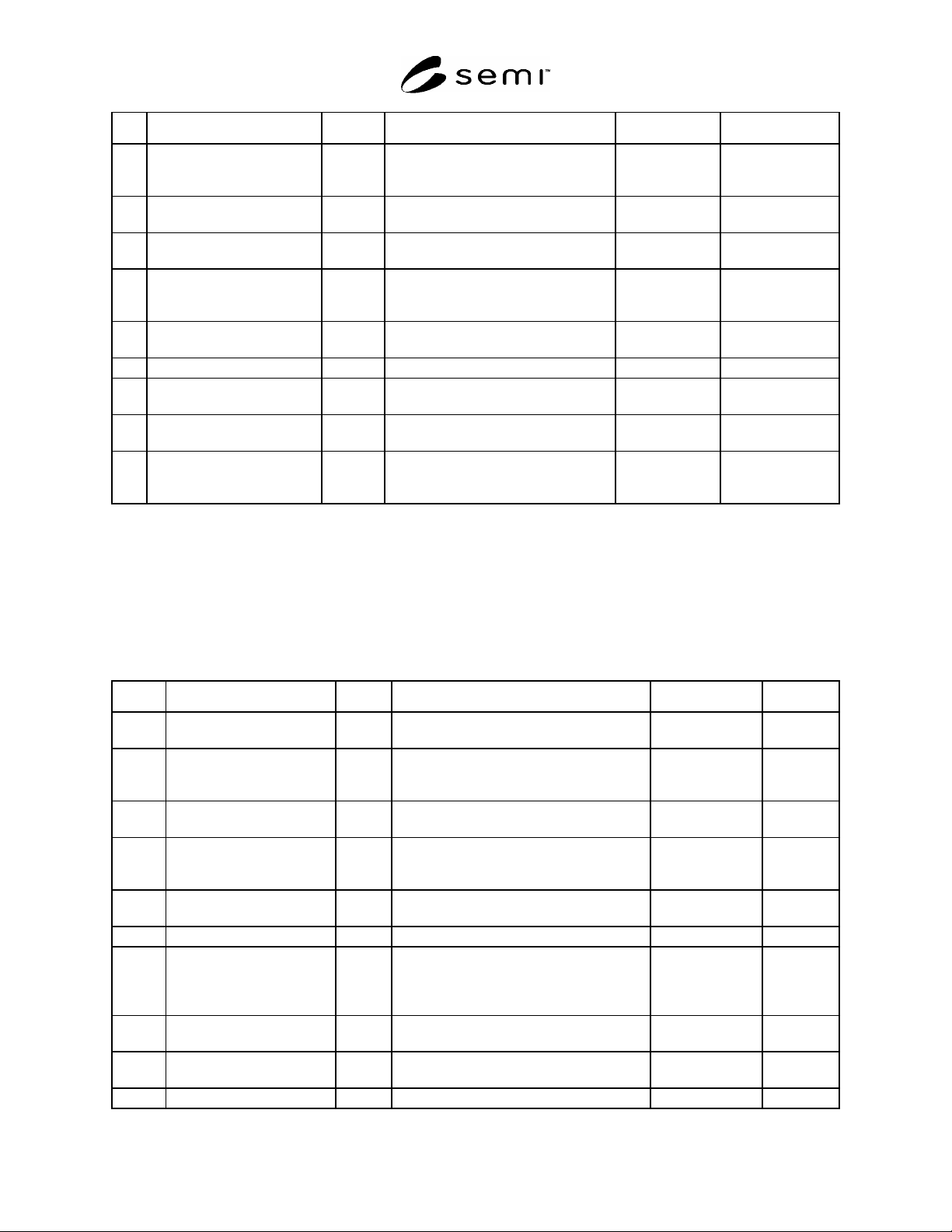
R1-5 Carrier Swap During Processing
R1-5.1 Multiple carriers are loaded to a batch processing tool that has buffering, after carriers are emptied, they are
removed and new empty carriers are loaded. In this example, it requires four carriers for a batch.
CJS = Control Job State, PJS = Process Job State
# Comment Dir Message CJS PJS
1 Create the process job. H->E PRJobCreateEnh (PRJobID=prj01_01,
Mtrl = CSA01,CSA02, CSA03,
CSA04, RecID=ILD1)
No state No state
2 H<-E PRJobCreateAck (PRJobID,
PRJobStatus)
In POOL
3 Request a control job.
Material out specification
maintains wafer order from
source carrier to destination
carrier.
H->E ControlJobCreate (CtrlJobID=cjf01_01,
ProcessingCtrlSpec= (prj01_01,
null,null), ProcessOrderMgmt =
ARRIVAL,
MtrlOutSpec=(((CSA01,null),(CSB01,
null)), ((CSA02, null), (CSB02,null)),
((CSA03, null), (CSB03,null)),
((CSA04, null), (CSB04,null))),
MaterialIn= (CSA01,CSA02, CSA03,
CSA04), StartMethod=AUTO)
4 Request accepted. H<-E ControlJobCreateAck
(CtrlJobID=cjf01_01, JobStatus)
QUEUED
5 No CJ in selected state so the
newly created job
immediately transitions.
H<-E Event (CJSELECTED,
CtrlJobID=cjf01_01)
SELECTED
6 A carrier for the selected
control job arrives.
H<-E Event (CARRIERIDREAD,
CID=CSA01)
7 The equipment recognizes it
and starts execution of the
ControlJob.
H<-E Event (ControlJobStart, cjf01_01) EXECUTING
8 ControlJob starts the
ProcessJob; begins loading
wafers to the processing boat.
H<-E Event (PRJOBSETUP, prj01_01) ACTIVE/SETUP
9 H<-E Event (CarrierEmpty,CSA01)
10 The next carrier arrives. H<-E Event (CARRIERIDREAD, CSA02)
11 H->E Rcommand (CarrierOut=CSA01)
As carriers are emptied they
are removed.
Steps 9 through 11 are repeated 3 more
times
SEMI E94-0705 © SEMI 2000, 2005 21
# Comment Dir Message CJS PJS
12 Material processing starts
after all material is in the
processing boat.
H<-E Event (PRJOBPROCESSING,
prj01_01)
ACTIVE/
PROCESSING
13 Output carriers begin to
arrive.
H<-E Event (CARRIERIDREAD,
CID=CSB01)
Until all output carriers
arrive.
Step 13 is repeated 3 more times
14 Equipment begins to load
output carriers.
H<-E Event (PROCESSINGCOMPLETE,
PRJob=prj01_01)
ACTIVE/
PROCESSING
COMPLETE
15 First output carrier is filled
with wafers.
H<-E Event (CarrierComplete=CSB04)
16 Host wants to get it. H->E Rcommand (CarrierOut=CSB04)
17 Gets rest of carriers. Steps 15 and 16 are repeated 3 more
times
18 H<-E Event (PRJOBCOMPLETE,
PRJob=prj01_01,)
No state
19 H<-E Event
(ControlJobCompleted=cjf01_01,
status=OK)
COMPLETE
R1-6 Using Cleaning Wafers
R1-6.1 For this scenario we assume a single wafer processing tool, such as an RIE. The tool has three fixed load
ports; two for product material, one for cleaning material. A cleaning wafer is run before the 1
st
and 13
th
wafer of
each carrier of product wafers. Show the load and unload of the cleaning wafers and the running of the ControlJob
for processing material. Note that control jobs do not provide functionality for dispositioning collateral material
consumed during processing (the cleaning wafers). The equipment is responsible for providing mechanisms to
determine when this collateral material has been consumed (should be replaced).
Step # Comment Dir Message CJS PJS
1 Remove the previously spent
wafers.
H<-E Event (ReadytoUnload, PortID=Cleaning,
CarrierID=CC01)
No state No state
2 After host picks up the spent
wafers, the equipment is
ready to load.
H<-E Event (ReadytoLoad, PortID=Cleaning)
3 Delivered material is
identified.
H<-E Event (CarrierIDRead, CarrierID=CC02)
4 Host directs carrier to be
moved to the wafer access
position.
H->E CMSProceedwithCarrier (CarrierID=CC02)
5 Create a job to run a
cleaning wafer.
H->E PRJobCreate (PRJobID=prj01_01, Mtrl =
ACleanWafer, RecID=CleaningProcess)
6 H<-E PRJobCreateAck (PRJobID, PRJobStatus) In POOL
7 Create the jobs for the first
12 wafers in the carrier
(PW1-12).
H->E PRJobDuplicateCreate (PRJobSpecList =
(prj01_02, PW1), (prj01_03, PW2),
…(prj01_13, PW12), RecID = P64ME5,
Start=AUTO, MtrlType=WAFER)
8 H<-E PRJobCreateAck (PRJobIDList,
PRJobStatus)
In POOL
9 Another cleaning wafer H->E PRJobCreate (PRJobID=prj01_14, Mtrl =
ACleanWafer, RecID=CleaningProcess)
10 H<-E PRJobCreateAck (PRJobID, PRJobStatus) In POOL
SEMI E94-0705 © SEMI 2000, 2005 22
Step # Comment Dir Message CJS PJS
11 The rest of the product
wafers
H->E PRJobDuplicateCreate (PRJobSpecList =
(prj01_15, PW13), (prj01_16, PW14),
…(prj01_27, PW25), RecID = P64ME5,
Start=AUTO, MtrlType=WAFER)
12 H<-E PRJobCreateAck (PRJobIDList,
PRJobStatus)
In POOL
13 Now the control job H->E CtrlJobCreate (CtrlJobID=cj01_01,
ProcessingCtrlSpecList = (prj01_01, null,
null), (prj01_02, null, null), …(prj01_27,
null, null), CarrierInputSpec = CP01, Start
= AUTO, ProcessOrderMgmt = LIST,
MtrlOutSpec = (CP01, null, CP01,null)
14 H<-E CtrlJobCreateAck (ID = cj01_01,
Status=OK )
QUEUED ->
SELECTED
15 H<-E Event (ReadytoLoad, PortID = P1)
16 H<-E Event (CarrierIDRead, CarrierID=CP01)
17 H->E CMSProceedwithCarrier (CP01)
18 H<-E Event (CtrlJobStart = cj01_01) EXECUTING
Host might not even have
these sent.
Lots of PRJob Start and End Events
19 H<-E Event (CtrlJobComplete = cj01_01) COMPLETED
20 H<-E Event (ReadytoUnload, CarrierID = CP01)
NOTICE: SEMI makes no warranties or representations as to the suitability of the standard set forth herein for any
particular application. The determination of the suitability of the standard is solely the responsibility of the user.
Users are cautioned to refer to manufacturer’s instructions, product labels, product data sheets, and other relevant
literature respecting any materials mentioned herein. These standards are subject to change without notice.
The user’s attention is called to the possibility that compliance with this standard may require use of copyrighted
material or of an invention covered by patent rights. By publication of this standard, SEMI takes no position
respecting the validity of any patent rights or copyrights asserted in connection with any item mentioned in this
standard. Users of this standard are expressly advised that determination of any such patent rights or copyrights, and
the risk of infringement of such rights, are entirely their own responsibility.
Copyright by SEMI® (Semiconductor Equipment and Materials
International), 3081 Zanker Road, San Jose, CA 95134. Reproduction of
the contents in whole or in part is forbidden without express written
consent of SEMI.