semi合集-English.pdf - 第7698页
SEMI T8-0698 E © SEMI 1998, 2004 7 APPENDIX 1 PLACEMENT OF DATA MATRIX CO DES ON DISPLAY SECTIONS OF FLAT PANEL DISP LAY SUBSTRATES NOTICE : This appe ndix was appro ved as an official part of SEMI T8, but the rec ommend…
SEMI T8-0698
E
© SEMI 1998, 2004 6
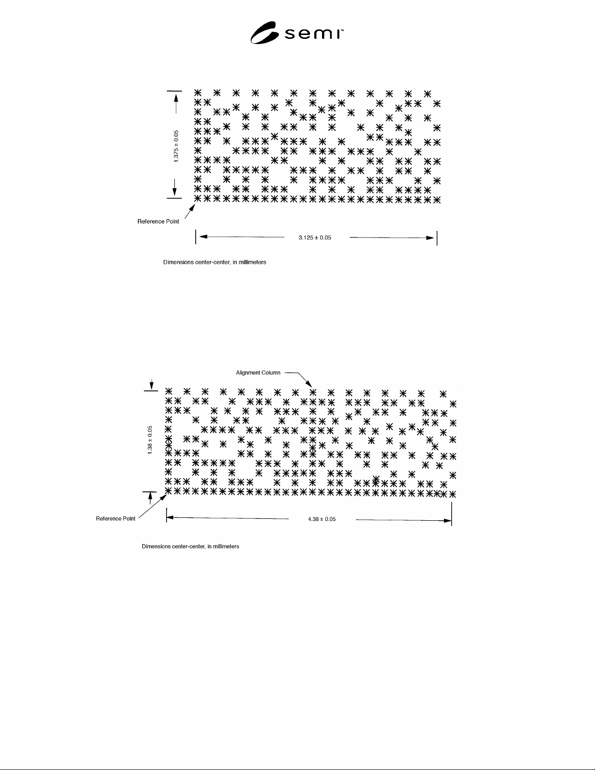
Figure 5
Data Matrix Code Field
Figure 6
Data Matrix Code Field
SEMI T8-0698
E
© SEMI 1998, 2004 7
APPENDIX 1
PLACEMENT OF DATA MATRIX CODES ON DISPLAY SECTIONS OF
FLAT PANEL DISPLAY SUBSTRATES
NOTICE: This appendix was approved as an official part of SEMI T8, but the recommendations in this appendix
are optional and are not required to conform to this standard.
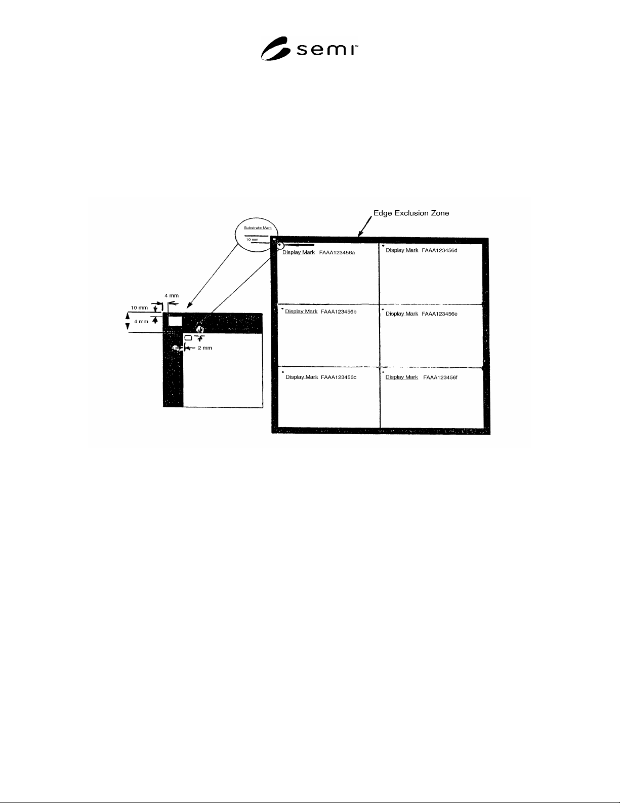
A1-1 The following suggests one way in which individual display sections could be marked while still a part of the
motherglass substrate. Figure A1-1 illustrates a six-up display layout on a 550 × 650 mm substrate
Figure A1-1
An Example of Mark Field Locations in Individual Display
Sections within a “Motherglass” Substrate
A1-2 The Substrate ID location falls within the edge exclusion area as detailed in Figure 4. In this example, all ID
fields are located on the back (non-pattern) surface. Placing them on the same surface as the substrate mark can
simplify ID reading during fabrication. Their location on the non-pattern surface could allow ID reading of the
outside surface of a display after assembly.
A1-3 The axes of the individual display IDs are parallel to the substrate ID axes. Each display ID is located adjacent
to a display corner. The locations of each ID field are given.
NOTE A1-1: This example does not constitute a recommended usage, but is intended to assist users in developing ID locations
suitable for their operations.

SEMI T8-0698
E
© SEMI 1998, 2004 8
NOTICE: SEMI makes no warranties or representations as to the suitability of the standards set forth herein for any
particular application. The determination of the suitability of the standard is solely the responsibility of the user.
Users are cautioned to refer to manufacturer's instructions, product labels, product data sheets, and other relevant
literature, respecting any materials or equipment mentioned herein. These standards are subject to change without
notice.
By publication of this standard, Semiconductor Equipment and Materials International (SEMI) takes no position
respecting the validity of any patent rights or copyrights asserted in connection with any items mentioned in this
standard. Users of this standard are expressly advised that determination of any such patent rights or copyrights, and
the risk of infringement of such rights are entirely their own responsibility.
Copyright by SEMI® (Semiconductor Equipment and Materials
International), 3081 Zanker Road, San Jose, CA 95134. Reproduction of
the contents in whole or in part is forbidden without express written
consent of SEMI.