semi合集-English.pdf - 第763页
SEMI E103-0704 © SEMI 2000, 2004 3 Figure 2 Front View o f Example Sin g le-Wafer Box and SWIF 6.7 SWIF Sensi n g — It is possible that the SWIF is not removed from the load port when single- wafer boxes are removed and …
SEMI E103-0704 © SEMI 2000, 2004 2
6 Requirements
6.1 System Components — A system that conforms to
this standard must include a box that holds one wafer
and that fits onto a SWIF.
6.2 Relevant FOUP Dimensions — The SWIF must
have all of the required bottom and front features and
be no larger than the maximum dimensions of a 13- or
25-wafer FOUP. However, this system (of single-wafer
box and SWIF) must have box placement sensing pads
as specified in SEMI E47.1 FOUP standards
Requirements Section 6.12. For example, the SWIF
must comply with dimensions r67, x53, y50, y51, y52,
y53, z41, z47 – z48, z47 + z49, and the upper limits on
x50 and y40 (as specified in SEMI E47.1) and with
dimension y33 (as specified in SEMI E62).
6.3 Optional Automation Features — Since the single-
wafer box and/or SWIF will usually be delivered
manually (possibly with a PGV), the SWIF is not
required to have the other automation features of the
FOUP such as the robotic handling flange on top or the
fork-lift flanges on the side (although this standard does
not forbid the SWIF from having such features).
6.4 SWIF Door — The SWIF must have a full FOUP-
size door (which surrounds the door of the single-wafer
box) that mates with a FIMS-compatible interface (as
specified in SEMI E62) to avoid contaminating the
environment on the equipment side of the FIMS
interface.
6.5 Wafer Position — When the FIMS door is opened
by the equipment, the end effector may only be able to
access the middle wafer slot (wafer 7 for a SWIF that
emulates a 13-wafer carrier, and wafer 13 for a SWIF
that emulates a 25-wafer carrier), because a surface
immediately behind the door may block access to the
other wafer slots. Thus, batch wafer handlers will
probably not work with this system.
6.6 Wafer Clearances — The clearance below the
middle wafer must be the same as the clearance below
the bottom wafer in an ordinary FOUP (z8 minus z6,
both from SEMI E1.9), and the clearance above the
middle wafer must be the same as the clearance above
the top wafer in an ordinary FOUP (z15 from SEMI
E1.9). These vertical clearances are defined in SEMI
E1.9 and SEMI E47.1 and apply throughout the wafer
set-down and extraction volumes for the middle wafer.
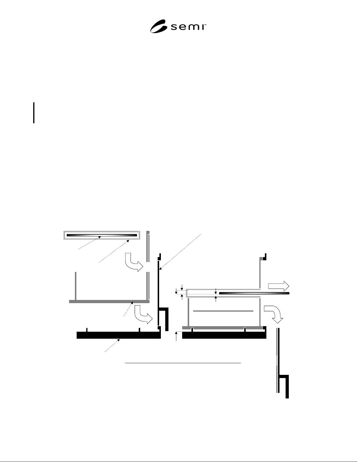
The horizontal clearances shown in Figure 10 of SEMI
E47.1 are also required. One possible example of such
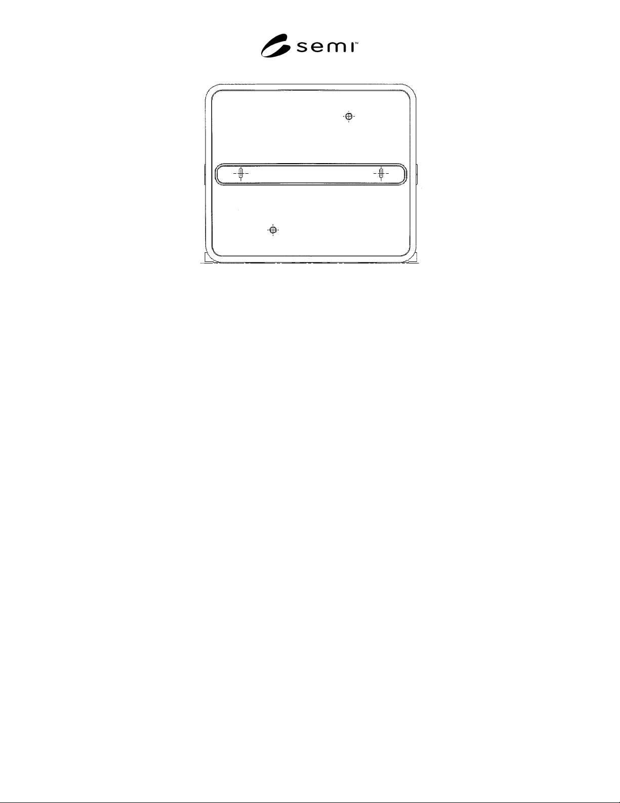
a system (of single-wafer box and SWIF) is shown in
Figures 1 and 2 (with vertical clearances indicated).
wafer
33 mm [z8 from SEMI E1.9]
–21 mm [z6 from SEMI E1.9]
= 12.0 mm minimum
11 mm [z44 from SEMI E47.1]
+ 33 mm [z8 from SEMI E1.9]
+ 10 mm [z12 from SEMI E1.9] × (6 or 12 wafers)
± 0.5 mm [z10 from SEMI E1.9]
= 164.0±0.5 mm (for wafer #13 in a 25-wafer FOUP)
or 104.0±0.5 mm (for wafer #7 in a 13-wafer FOUP)
13.0 mm minimum
[z15 from SEMI E1.9]
single-wafer box
single wafer interface (SWIF)
equipment load port
FIMS port
11 mm [
z
44 from
SEMI
E47.1
]
+ 33 mm [
z
8 from
SEMI E1.9
]
+ 10 mm [
z
12 from
SEMI E1.9
] × (6 or 12 wafers)
± 0.5 mm [
z
10 from
SEMI E1.9
]
= 164.0 ± 0.5 mm (for wafer
#
13 in a 25-wafer FOUP)
or 104.0 ± 0.5 mm (for wafer
#
7 in a 13-wafer FOUP)
Figure 1
Side View of Example Single-Wafer Box and SWIF on a Load Port with a FIMS Interface
SEMI E103-0704 © SEMI 2000, 2004 3
Figure 2
Front View of Example Single-Wafer Box and SWIF
6.7 SWIF Sensing — It is possible that the SWIF is not
removed from the load port when single-wafer boxes
are removed and replaced on the SWIF. However,
when the single-wafer box is removed from the SWIF,
all of the carrier sensing pads (defined in Section 6.6 of
SEMI E1.9) on the bottom of the SWIF must be raised
(so that the load port can sense a change of carriers by
its carrier placement sensor, if any). However, in order
to ensure that the SWIF triggers most optical carrier
presence detectors on the load port, the SWIF (without
a single-wafer box) must block any line of sight
through a volume consisting of the smallest cylindrical
section that contains all of the wafer pick-up volumes
(defined in SEMI E1.9) of the corresponding FOUP
(defined in SEMI E47.1). Note that this standard does
not prevent the use of other kinds of carrier presence
detectors (such as sensors that detect weight on the load
port).
7 Related Documents
7.1 SEMI Standards
SEMI E15.1 — Specification for 300 mm Tool Load
Port
SEMI E57 — Mechanical Specification for Kinematic
Couplings Used to Align and Support 300 mm Wafer
Carriers
SEMI E63 — Mechanical Specification for 300 mm
Box Opener/Loader to Tool Standard (BOLTS-M)
Interface
SEMI E72 — Specification and Guide for 300 mm
Equipment Footprint, Height, and Weight
SEMI E92 — Specification for 300 mm Light Weight
and Compact Box Opener/Loader and Tool-Interface
Standard (BOLTS-Light)
SEMI M31 — Provisional Mechanical Specification for
Front-Opening Shipping Box Used to Transport and
Ship 300 mm Wafers
SEMI S8 — Safety Guidelines for Ergonomics/ Human
Factors Engineering of Semiconductor Manufacturing
Equipment
NOTICE: Unless otherwise indicated, all documents
cited shall be the latest published versions.
NOTICE: SEMI makes no warranties or representa-
tions as to the suitability of the specification set forth
herein for any particular application. The determination
of the suitability of the specification is solely the
responsibility of the user. Users are cautioned to refer
to manufacturer’s instructions, product labels, product
data sheets, and other relevant literature respecting any
materials mentioned herein. These specifications are
subject to change without notice.
The user’s attention is called to the possibility that
compliance with this specification may require use of
copyrighted material or of an invention covered by
patent rights. By publication of this specification,
SEMI takes no position respecting the validity of any
patent rights or copyrights asserted in connection with
any item mentioned in this specification. Users of this
specification are expressly advised that determination
of any such patent rights or copyrights, and the risk of
infringement of such rights, are entirely their own
responsibility.

SEMI E103-0704 © SEMI 2000, 2004 4
RELATED INFORMATION 1
APPLICATION NOTES
NOTICE: This related information is not an official part of SEMI E103 but was approved for publication by full
letter ballot procedures on July 28, 2000.
R1-1
R1-1.1 In fabs in which this system (of single-wafer box and SWIF) is used, equipment should have control
software algorithms that prevent end effectors and wafer slot mappers from entering the carrier except in the
clearances around the middle wafer (defined in Section 6.2) when the presence of this system is detected. A variety
of methods for differentiating the system from ordinary FOUPs are possible.
R1-1.2 Using sensors, equipment can differentiate the system (of single-wafer box and SWIF) from ordinary
FOUPs. For example, sensors below the info pad B location on the load port and on the FIMS door (opposite the
seal zones or the reserved spaces for vacuum application on the box door) could indicate that the carrier type is an
open cassette but with a FOUP door, together implying the presence of this system (of a single-wafer box and
SWIF). Note that such sensors on the load port are not currently specified in any SEMI standard.
R1-1.3 Carrier ID tags can inform the equipment that the load port holds this system (of single-wafer box and
SWIF) instead of an ordinary FOUP.
R1-1.4 Messages from the host computer system can inform the equipment that the load port holds this system (of
single-wafer box and SWIF) instead of an ordinary FOUP.
NOTICE: SEMI makes no warranties or representations as to the suitability of the specification set forth herein for
any particular application. The determination of the suitability of the specification is solely the responsibility of the
user. Users are cautioned to refer to manufacturer’s instructions, product labels, product data sheets, and other
relevant literature respecting any materials mentioned herein. These specifications are subject to change without
notice.
The user’s attention is called to the possibility that compliance with this specification may require use of
copyrighted material or of an invention covered by patent rights. By publication of this specification, SEMI takes
no position respecting the validity of any patent rights or copyrights asserted in connection with any item mentioned
in this specification. Users of this specification are expressly advised that determination of any such patent rights or
copyrights, and the risk of infringement of such rights, are entirely their own responsibility.
Copyright by SEMI® (Semiconductor Equipment and Materials
International), 3081 Zanker Road, San Jose, CA 95134. Reproduction o
f
the contents in whole or in part is forbidden without express written
consent of SEMI.