semi合集-English.pdf - 第4078页
SEMI F56-0600 © SEMI 2000 8 Table 1 Data S heet Data Shee t 1 Data fr om Ste ady State Power Supply Effects Colum n A Column B Column C Column D Column E Column F Colum n G Column H Colum n L Column M Data Pnts MFC Setpo…
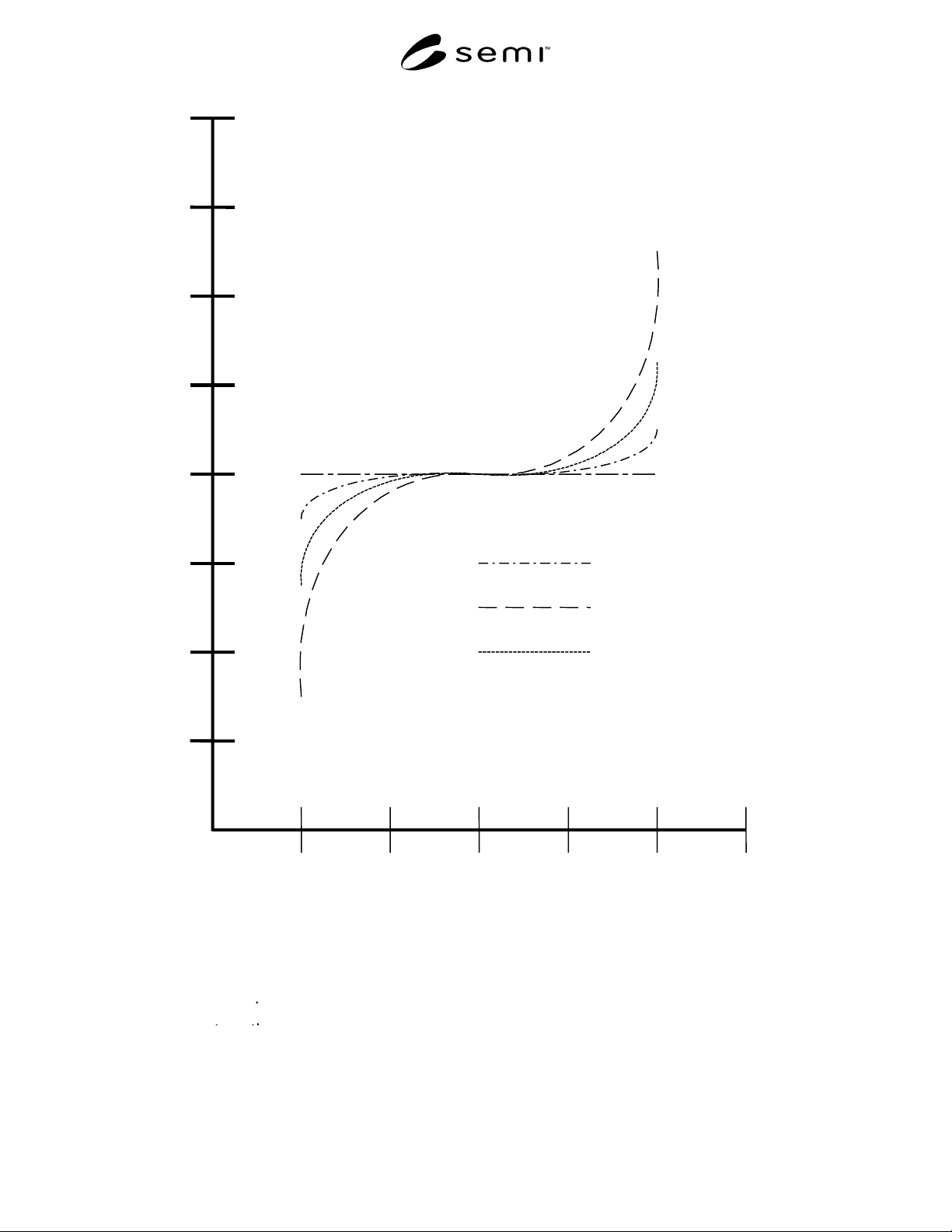
SEMI F56-0600 © SEMI 20007
Span (Actual Flow)
Span of MFC
ZERO
Ideal Response
0
Positive Voltage Variation
-3
-2
-1
0
1
2
3
Flow Changes (%FS)
A
similar plot would be obtained:
Zero and span effects as a result of varying the negative power
l
zero and span effects as a results of varying both power supplies
tth
Figure 4
Data Plots
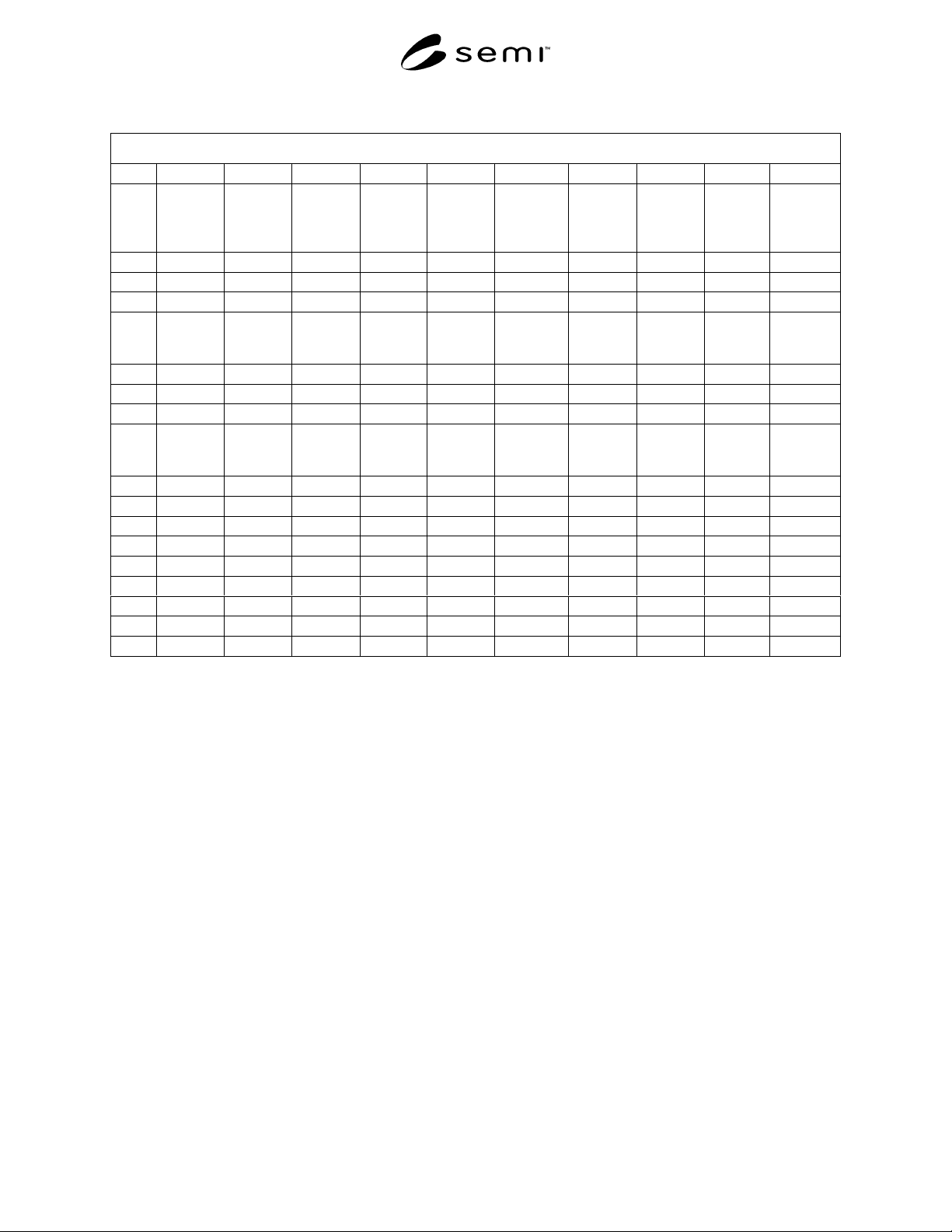
SEMI F56-0600 © SEMI 2000 8
Table 1 Data Sheet
Data Sheet 1 Data from Steady State Power Supply Effects
Column A Column B Column C Column D Column E Column F Column G Column H Column L Column M
Data
Pnts
MFC
Setpoint
MFC
Indicated
Flow (V)
Flow
Standard
Output
(V)
Positive
Power
Supply
Level (V)
Negative
Power
Supply
Level (V)
Power
Supply
Current
Level (mA)
MFC
Indicated
Flow %FS
Flow
Standard
%FS
Positive
Power
Supply
Var. (%)
Negative
Power
Supply
Var. (%)
10 0 0 15-15 30 0 0 0 0
20 0 0 15-15 30 0 0
30 0 0 15-15 30 0 0
.
.
.
4 0 0.015 0 15.15 -15 30 0.3 0 1.0 0
5 0 0.010 0 15.15 -15 30 0.3 0
6 0 0.010 0 15.15 -15 30 0.3 0
.
.
.
7 0 0.015 0 14.85 -15 30 0.3 0 -1.0 0
8 0 0.010 0 14.85 -15 30 0.2 0
9 0 0.015 0 14.85 -15 30 0.3 0
.
10 0 0.010 0 15 -15.15 30 0.3 0 0 1.0
11 0 0.010 0 15 -15.15 30 0.3 0
12 0 0.010 0 15 -15.15 30 0.3 0
.
13 0 0.005 0 15 -14.85 30 0.1 0 0 -1.0
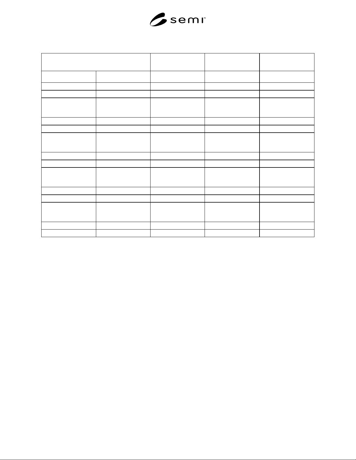
SEMI F56-0600 © SEMI 20009
Table 2 Zero and Span Effects as a Function of Steady-State Power Supply
Power Supply Voltage Change
(% of reference)
Change in Zero
of MFC (%FS)
Span of MFC
(%FS)
Span - Actual Flow
(%FS)
Positive Negative
00000
-1 0 0.25 99.8 100.0
.
.
.
.
.
.
.
.
.
.
.
.
.
.
.
00000
-1 0
.
.
.
.
.
.
00
0+1
.
.
.
.
.
.
00
1-1
.
.
.
.
.
.
00
11
NOTICE: SEMI makes no warranties or representations as to the suitability of the test method set forth herein for
any particular application. The determination of the suitability of the test method is solely the responsibility of the
user. Users are cautioned to refer to manufacturer’s instructions, product labels, product data sheets, and other rele-
vant literature respecting any materials mentioned herein. These test methods are subject to change without notice.
The user’s attention is called to the possibility that compliance with this test method may require use of copyrighted
material or of an invention covered by patent rights. By publication of this test method, SEMI takes no position
respecting the validity of any patent rights or copyrights asserted in connection with any item mentioned in this test
method. Users of this test method are expressly advised that determination of any such patent rights or copyrights,
and the risk of infringement of such rights, are entirely their own responsibility.
Copyright by SEMI® (Semiconductor Equipment and Materials
International), 3081 Zanker Road, San Jose, CA 95134. Reproduction o
f
the contents in whole or in part is forbidden without express written
consent of SEMI.