semi合集-English.pdf - 第4991页
SEMI M13-1103 © SEMI 1988, 2003 3 Table 3 Code Character Location CharacterStyle Parameter Code Definit ion 1 Alpha/Numeric 2 Alpha/Numeric 3 Alpha/Numeric 4 Alpha/Numeric 5 Alpha/Numeric 6 Alpha/Numeric 7 Alpha/Numeric …
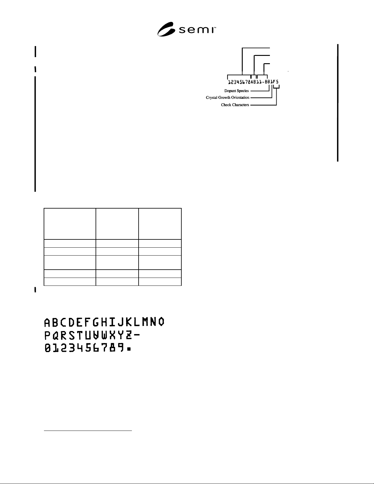
SEMI M13-1103 © SEMI 1988, 2003 2
identification code (see SEMI AUX001
1
) (See Figure 2
and Table 3.)
NOTE 1: In the absence of a character at any assigned
location, a dash (-) must be used.
6.2 Code Field Location and Dimensions — The
alphanumeric code field shall be located on the front
surface of the wafers (see Figures 3 and 4 for location
and dimensions of the alphanumeric code field for
flatted and notched wafers, respectively).
6.3 Character Alignment
6.3.1 Character Skew — the maximum allowable angle
between the character baseline and a line parallel with
the bottom of the character window shall be 3 degrees
(see Figure 5).
6.3.2 Maximum Character Misalignment — the
maximum adjacent character misalignment, R
adj
, shall
be 0.23 mm (see Figure 6), and the maximum line
character misalignment, R
line
,
,
shall be 0.46 mm (see
Figure 7).
Table 1 Character Dimensions
Character 100 mm, 125 mm,
and 150 mm
Flatted Wafers,
mm
150 mm and 200
mm Notched
Wafers, mm
Height 0.812 ± 0.025 1.624 ± 0.025
Width 0.406 ± 0.025 0.812 ± 0.025
Thickness 0.100 ± 0.050 0.200 + 0.025 or
– 0.150
Spacing 0.710 ± 0.025 1.420 ± 0.025
Minimum Separation 0.104 0.308
NOTE 1: The diagonal thickness of the letter “N” is 0.138 ± 0.05
mm.
Table 2 Standard Character Set
1
SEMI AUX001, List of Wafer Supplier Identification Codes,
available from SEMI web site: www.semi.org.
Identification Number 12345678
Wafer Supplier Identification See SEMI AUX001
2
Resistivity Identification 11.8
Ω·cm
Dopant Species Boron
Crystal Growth Orientation [111]
Check Characters (F5) Machine input for code acceptance
Identification Number
Wafer Supplier Identification
Resistivity Identification
Figure 2
Example of Code
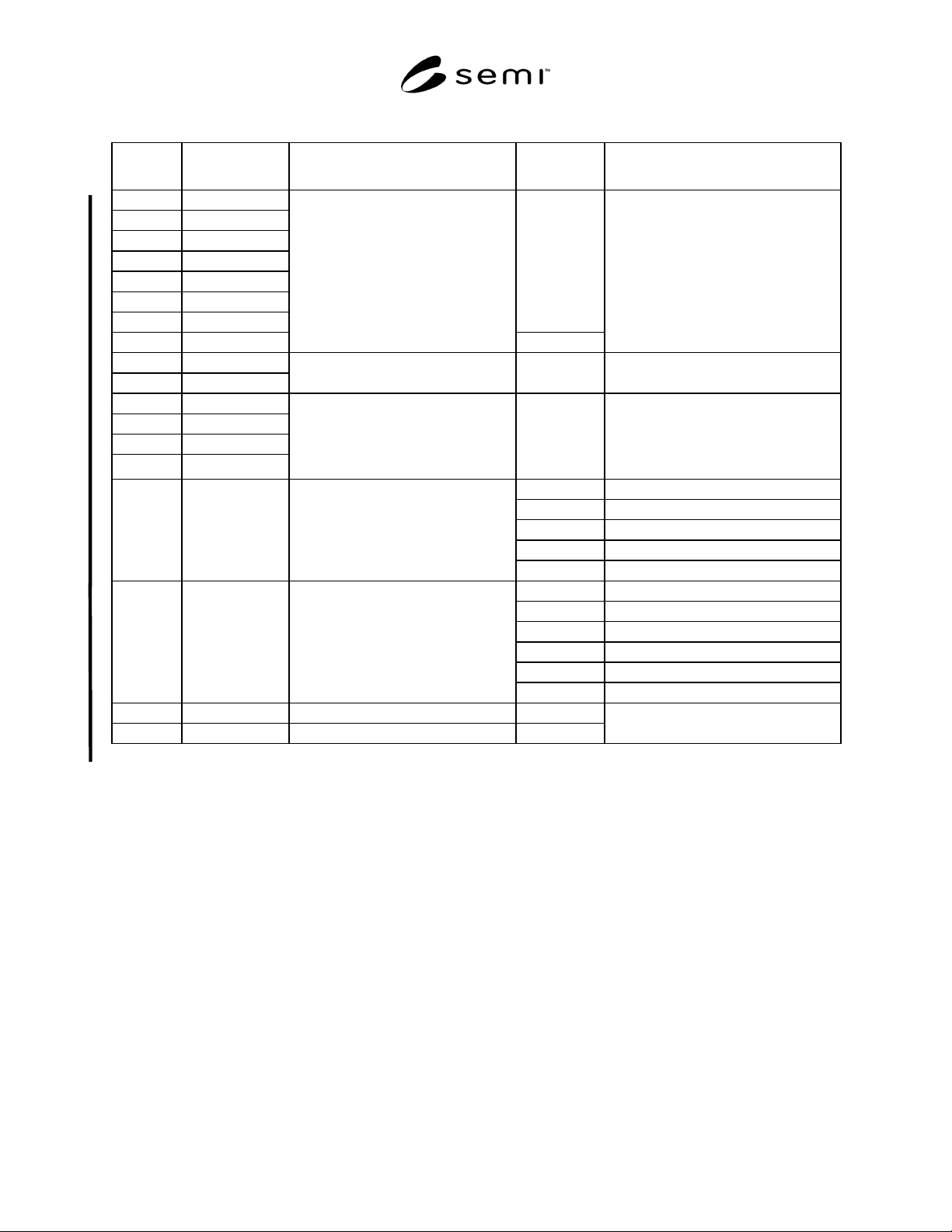
SEMI M13-1103 © SEMI 1988, 2003 3
Table 3 Code
Character
Location
CharacterStyle Parameter Code Definition
1 Alpha/Numeric
2 Alpha/Numeric
3 Alpha/Numeric
4 Alpha/Numeric
5 Alpha/Numeric
6 Alpha/Numeric
7 Alpha/Numeric
A through Z
and
0 through 9
8 Numeric Only
IDENTIFICATION NUMBER
0 through 9
Supplier-Assigned (See NOTE 1.)
9 Alpha Only
10 Alpha Only
SUPPLIER IDENTIFICATION A through Z (see SEMI AUX001 and NOTE 1.)
11 Numeric Only
12 Numeric Only
13 Numeric Only
14 Numeric Only
RESISTIVITY IDENTIFICATION
0 through 9
and .(period)
Resistivity (Ω·cm) identification is
assigned by supplier, expressed as a
whole number or as a mixed number
with a decimal fraction. No accuracy is
implied. (See NOTE 1.)
B Boron
F Phosphorous
A Arsenic
S Antimony
15 Alpha Only DOPANT SPECIES
– not identified
0 [100]
1 [111]
2 [110]
3 [011]
5 [511]
16
Numeric Only
CRYSTAL GROWTH
ORIENTATION
– not identified
17 Alpha Only CHECK CHARACTER A
17
A through H
18 Numeric Only CHECK CHARACTER A
18
0 through 7
Error-Detecting Method
(see Section 7)
NOTE 1: In the absence of information at any assigned location, a dash (–) must be used.
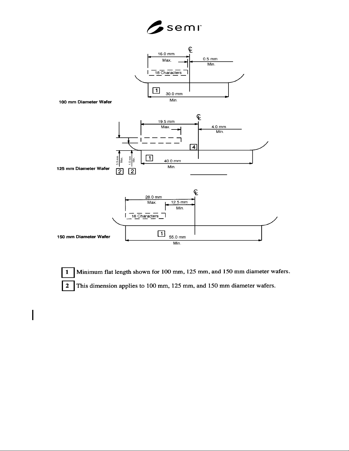
SEMI M13-1103 © SEMI 1988, 2003 4
Figure 3
Code Field Location for Flatted Wafers