semi合集-English.pdf - 第4847页
SEMI M1-0305 © SEMI 1978, 2005 23 NOTE: The pin shown in the outline on this figur e is us ed to align the notched wafer in a fixture during use. The pin is also used to ref erence the not ched wafer during testing for n…
SEMI M1-0305 © SEMI 1978, 2005 22
6.6 Dimensional Characteristics
6.6.1 Dimensions and Fiducials — The wafers shall conform to the dimensions, dimensional tolerances, and
fiducial (flat or notch) characteristics and locations as specified in the purchase order.
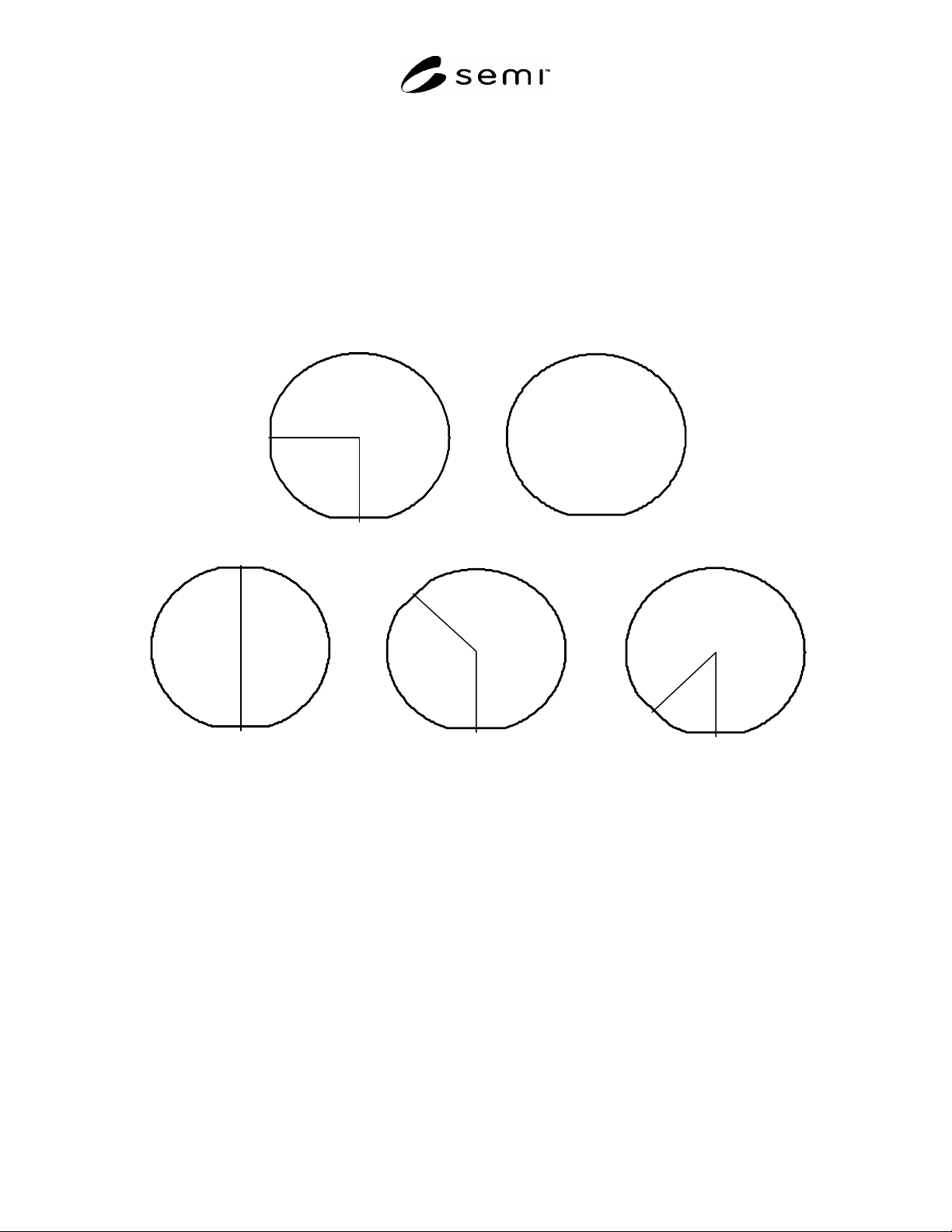
6.6.1.1 Where secondary flats are specified, they shall be located as shown in Figure 4.
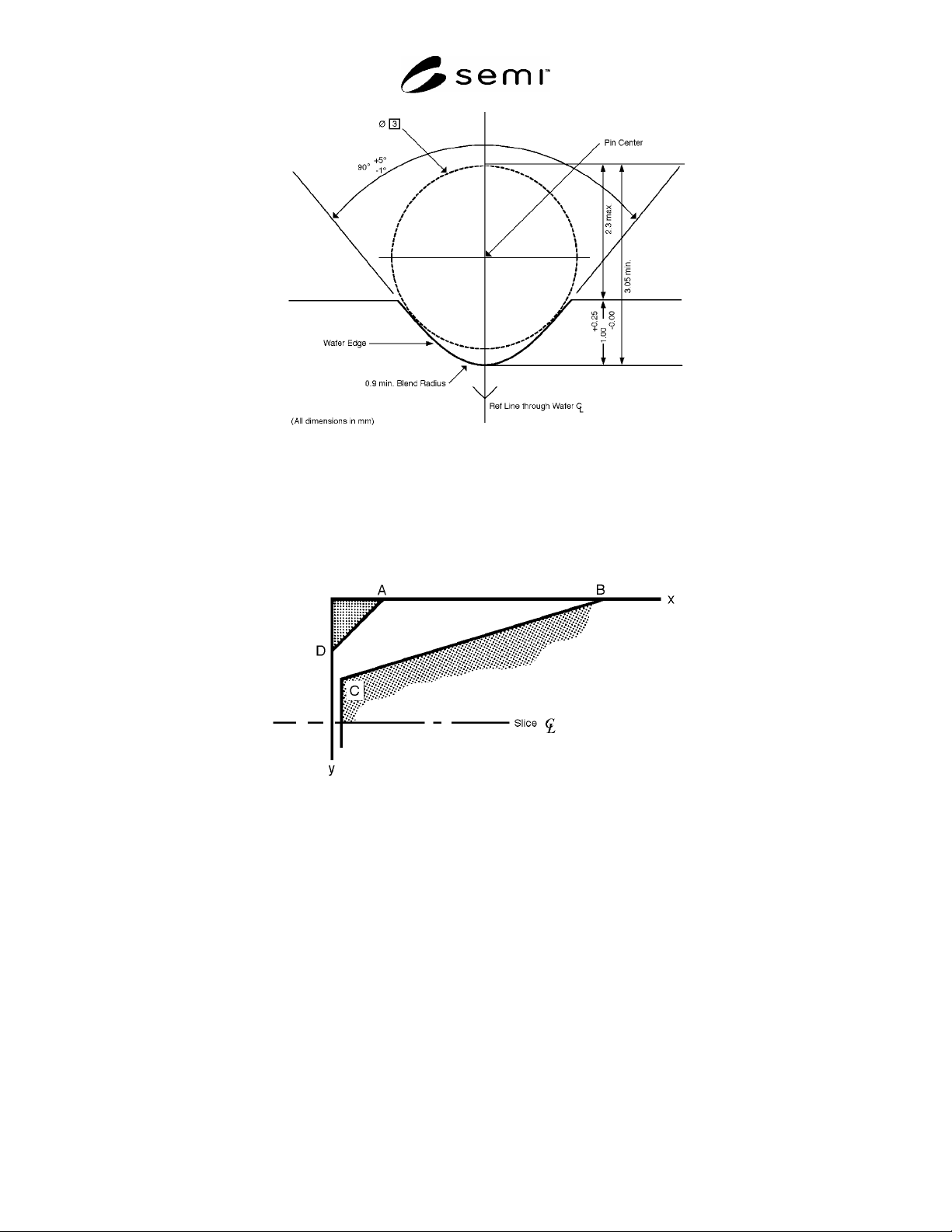
6.6.1.2 Where notches are specified, they shall conform to the dimensions in Figure 5.
6.6.2 Edge Profile — The edge profile of edge-profiled wafers shall conform to the following requirements at all
points on the wafer periphery (except interior portions of notches, if present).
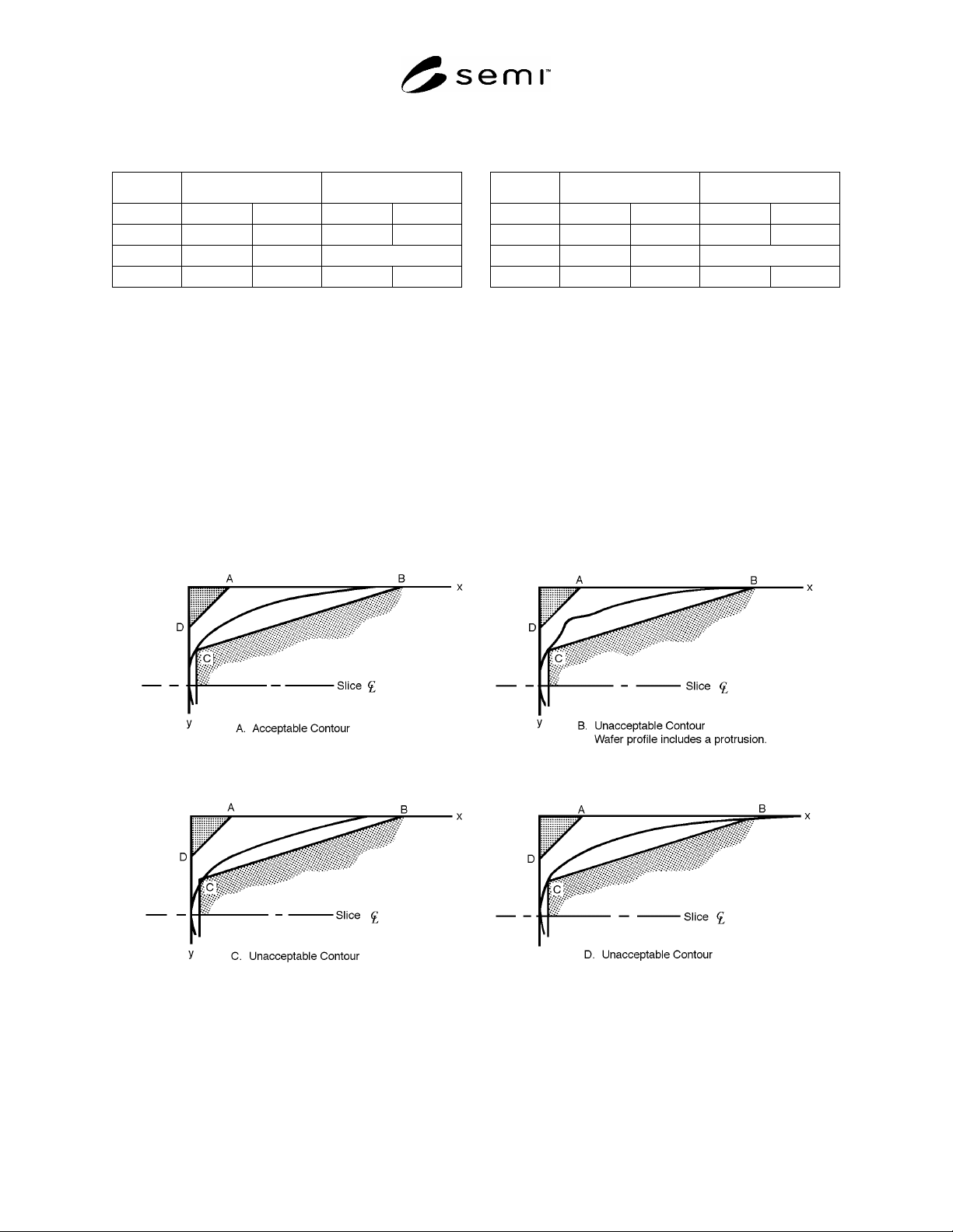
6.6.2.1 The SEMI Wafer Edge Profile Template is shown in Figure 6. There are two sets of dimensions for the
template: T/3 and T/4, where T is the nominal thickness of the wafer (see Tables 4 through 9 for values of the
nominal thickness for various wafer categories).
90
CW
180 CW
135 CW
45 CW
a. (
100) p-type b. (111) p-type
c. (100) n-type d. (100) n-type e. (111) n-type
(wafers 125 mm diameter or less) (150 mm diameter wafers only)
NOTE 1: Secondary flat location for 150 mm diameter (100) n-type wafers changed from configuration c to configuration d
effective January 1, 1990.
NOTE 2: The angular position of the center point of the secondary flat is given in Tables 4 through 6 both in terms of the
clockwise angle from the primary flat, located at the bottom of each figure, to the secondary flat and the angle,
, from the
positive x-axis of the wafer coordinate system as defined by SEMI M20 (at 3 o’clock) to the secondary flat.
Figure 4
Secondary Flat Locations
SEMI M1-0305 © SEMI 1978, 2005 23
NOTE: The pin shown in the outline on this figure is used to align the notched wafer in a fixture during
use. The pin is also used to reference the notched wafer during testing for notch dimensions and
dimensional tolerances. The notch dimensions shown in the figure assume a 3 mm diameter for this
alignment pin.
Figure 5
Notch Dimensions
NOTE 1: The figure is not to scale
NOTE 2: Only one-half of the template is shown; the wafer surface is aligned with the x-axis, and the outermost radial portion of
the edge contour is aligned with the y-axis. The template in this figure is not intended for use in measuring wafer thickness.
NOTE 3: Constant radius profile with blended, tangential front and back surface intercepts is preferred for ease of manufacture
and reduced particle and chip generation.
NOTE 4: The x- and y-axes in this template do not correspond with the x- and y-axes in the wafer coordinate system defined in
SEMI M20.
Figure 6
SEMI Wafer Edge Profile Template
SEMI M1-0305 © SEMI 1978, 2005 24
Table 3 Wafer Edge Profile Template Coordinates (See Figure 6)
T/3 Wafer Edge Profile Template
Point x
#1
y
#1
A 0.0030 in.
76 m
0.00 in.
0 m
B 0.0200 in.
508 m
0.00 in.
0 m
C 0.0020 in.
50 m
T/3
#2
D 0.00 in.
0 m
0.0030 in.
76 m
T/4 Wafer Edge Profile Template
Point x
#1
y
#1
A 0.0047 in.
120 m
0.00 in.
0 m
B 0.0200 in.
508 m
0.00 in.
0 m
C 0.0040 in.
100 m
T/4
#2
D 0.00 in.
0 m
0.0020 in.
50 m
#1
For referee purposes, U.S. Customary units are to be used for 2 and 3 in. diameter wafers SI units are to be used for all other wafers.
#2
For the value of this coordinate, see the specifications for the appropriate wafer category in Tables 4 through 9.
6.6.2.2 The coordinates for the two templates are given in Table 3. Note that this coordinate system differs from
that in SEMI M20 in that the origin is at the wafer edge instead of the wafer center and the y-axis is positive in the
downward direction toward the wafer median plane instead of being in the plane of the wafer surface. If the
nominal edge exclusion, EE, is 1 mm or greater, the edge profile will not extend into the fixed quality area.
6.6.2.3 When the wafer is aligned with the Template so that the x-axis of the template is coincident with the wafer
surface and the y-axis of the template is tangent with the outermost radial portion of the profile, the wafer edge
profile must be contained within the clear region of the template. (See Figure 7 for examples of acceptable and
unacceptable edge profiles.)
6.6.2.4 No sharp points or protrusions are permitted anywhere on the wafer edge profile.
6.6.2.5 Cosmetic attributes of the edge profile are not covered by this specification. They shall be agreed upon
between supplier and customer.
Figure 7
Examples of Acceptable and Unacceptable Wafer Edge Profiles