semi合集-English.pdf - 第3638页
SEMI E139.1-0705 © SEMI 2005 14 Figure 11 Manifest 8.1.3 XML simpleTypes 8.1.3.1 Table 11 describes each sim pleType added to the XML schema for the Manifest. Table 14 simpleTy pes In The PDE Schema Type Description UUID…
SEMI E139.1-0705 © SEMI 2005 13
o Convert the modified PDE element to its canonical form according to W3C recommendation xml-c14n
without comments (that is, the “with comments” option is not used). This yields an octet stream encoded in
UTF-8.
o Apply the MD5 algorithm to the resulting octet stream to compute the checksum.
7.2.2.2.4 The resulting checksum value can be used as needed. For example, if a new PDE is being created, the
value may be placed into the checksum element. For an existing PDE, the value may be compared with the existing
value of the checksum element to determine if the content is unchanged.
7.2.2.3 PDEbody BodyChecksum
7.2.2.3.1 The format of an external PDEbody is determined by the equipment supplier. In this case, the entire
PDEbody content as contained within TransferContainer shall be included in the checksum calculation process. The
calculation method for the bodyChecksum attribute of the PDEbodyReference element is MD5 as specified by the
E139 RaP standard.
7.2.3 XML Schema
7.2.3.1 All PDE instance documents shall conform to the XML schema document named:
E139-1.V0705.RaP.PDE.xsd
7.2.3.2 The contents of the above-mentioned schema document constitute a core part of this specification. This
schema document should be provided with this document.
7.2.3.3 In addition, all PDE instance documents shall conform to all requirements related to the PDE content as
specified in SEMI E139.
8 Manifest Schema Definition
8.1 Manifest Mapping to XML
8.1.1 This section describes how the Manifest definition from SEMI E139 is mapped to XML. The descriptions in
this section are provided to support and explain the XML schema document (attached, see ¶8.2). This section
contains no requirements. Specific requirements are included in ¶8.2.
8.1.2 Manifest Class
8.1.2.1 SEMI E139 does not represent the Manifest in UML. To facilitate creation of the Manifest schema, the
Manifest itself is treated as a single class containing an unordered sequence of Entries.
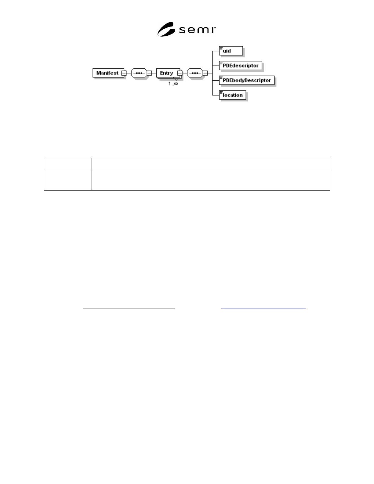
8.1.2.2 The first two columns of the Translation Table for this Manifest class (Table 13) hold little information
because this class was not explicitly defined in SEMI E139. However, the second two columns describe the XML
form of the Manifest class. Figure 11 shows the XML form of the Manifest.
Table 13 Translation Table For Manifest Class
Attribute or Role
Name
UML Type
XML Element or Attribute (or
Reference)
XML Name/Type
<none> <none> element Manifest (complexType)
<none> <none> element Entry (complexType)
<none> UUID element uid (simpleType UUID)
<none> String element PDEdescriptor (simpleType xs:string)
<none> String element PDEbodyDescriptor (simpleType xs:string)
<none> String element location (simpleType xs:string)
SEMI E139.1-0705 © SEMI 2005 14
Figure 11
Manifest
8.1.3 XML simpleTypes
8.1.3.1 Table 11 describes each simpleType added to the XML schema for the Manifest.
Table 14 simpleTypes In The PDE Schema
Type Description
UUID Holds a standard 36-character uuid string. The pattern is defined as five groups of characters, each
separated by the “-“ character. Here is an example value in UUID format: “44BBA855-CC51-11CF-
AAFA-00AA00B6015C”.
8.2 Requirements For Manifest Schema
8.2.1 This section contains all requirements specified for the PDE Schema. ¶8.1 above is included for
documentation purposes.
8.2.2 All Manifest instance documents shall conform to the XML schema document named:
E139-1.V0705.RaP.Manifest.xsd
8.2.3 The contents of the above-mentioned schema document constitute a core part of this specification. This
schema document should be provided with this document.
8.2.4 In addition, all Manifest instance documents shall conform to all requirements related to the Manifest content
as specified in SEMI E139.
9 Related Documents
Rivest, Ronald, The MD5 Message-Digest Algorithm,
IETF RFC: 1992 http://www.ietf.org/rfc/rfc1321.txt.
NOTICE: SEMI makes no warranties or representations as to the suitability of the standards set forth herein for any
particular application. The determination of the suitability of the standard is solely the responsibility of the user.
Users are cautioned to refer to manufacturer's instructions, product labels, product data sheets, and other relevant
literature, respecting any materials or equipment mentioned herein. These standards are subject to change without
notice.
By publication of this standard, Semiconductor Equipment and Materials International (SEMI) takes no position
respecting the validity of any patent rights or copyrights asserted in connection with any items mentioned in this
standard. Users of this standard are expressly advised that determination of any such patent rights or copyrights, and
the risk of infringement of such rights are entirely their own responsibility.
Copyright by SEMI® (Semiconductor Equipment and Materials
International), 3081 Zanker Road, San Jose, CA 95134. Reproduction of
the contents in whole or in part is forbidden without express written
consent of SEMI.

SEMI E142-0705 © SEMI 2005 1
SEMI E142-0705
SPECIFICATION FOR SUBSTRATE MAPPING
This specification was technically approved by the Global Information & Control Committee and is the direct
responsibility of the North American Information & Control Committee. Current edition approved by the
North American Regional Standards Committee on December 10, 2004. Initially available at www.semi.org
January 2005; to be published March 2005.
NOTICE: The designation of SEMI M55 was updated during the 0705 publishing cycle to reflect the creation of
SEMI E142.1.
1 Purpose
1.1 This document defines the data items that are required to report, store and transmit map data for substrates such
as wafers, frames, strips and trays.
2 Scope
2.1 This version of the document applies to the substrate types; wafers, frames, strips and trays.
2.2 This document addresses assembly and packaging including the testing of semiconductor devices.
NOTICE: This standard does not purport to address safety issues, if any, associated with its use. It is the
responsibility of the users of this standard to establish appropriate safety and health practices and determine the
applicability of regulatory or other limitations prior to use.
3 Limitations
3.1 This document does not address the transmission, file naming conventions, storage or archiving of substrate
maps. These will be addressed in sub-documents of this specification.
4 Referenced Standards
4.1 SEMI Standards
SEMI E39 — Object Services Standard; Concept, Behavior and Services
NOTICE: Unless otherwise indicated, all documents cited shall be the latest published versions.
5 Terminology
5.1 Definitions
5.1.1 bottom side — the bottom side of the substrate as defined in the corresponding Appendix (Appendix 1, 2,
or 3).
5.1.2 device — the unit to which the device status code in the map is assigned including, but not limited to: die on a
wafer, multi-chip modules, and packages.
5.1.3 map — a two-dimensional array of bin codes derived from electrical test data of a substrate including, but not
limited to: wafer, tray, strip, or tape.
5.1.4 substrate — any carrier of a two-dimensional array of devices including, but not limited to: wafers, trays,
strips, tape, panels, or boards.
5.1.5 top side — the top side of the substrate as defined in the corresponding Appendix for that substrate
(Appendix 1, 2, or 3).
6 Requirements
6.1 This standard defines the data items that are required in a substrate map. This standard places no special
requirements on the file naming conventions, storage, or archiving of substrate maps.