semi合集-English.pdf - 第6486页
SEMI G78-0699 © SE MI 1999 19 A1- 1 .18.7 T ip s for gr aph ma king : • Add gridlines across the X-axis to separate wafers. • Print all graphs (X and Y, different lots , different probers) w ith the same scale in X and Y…
SEMI G78-0699 © SEMI 1999 18
A1-1.15 Step 13 — Calculate
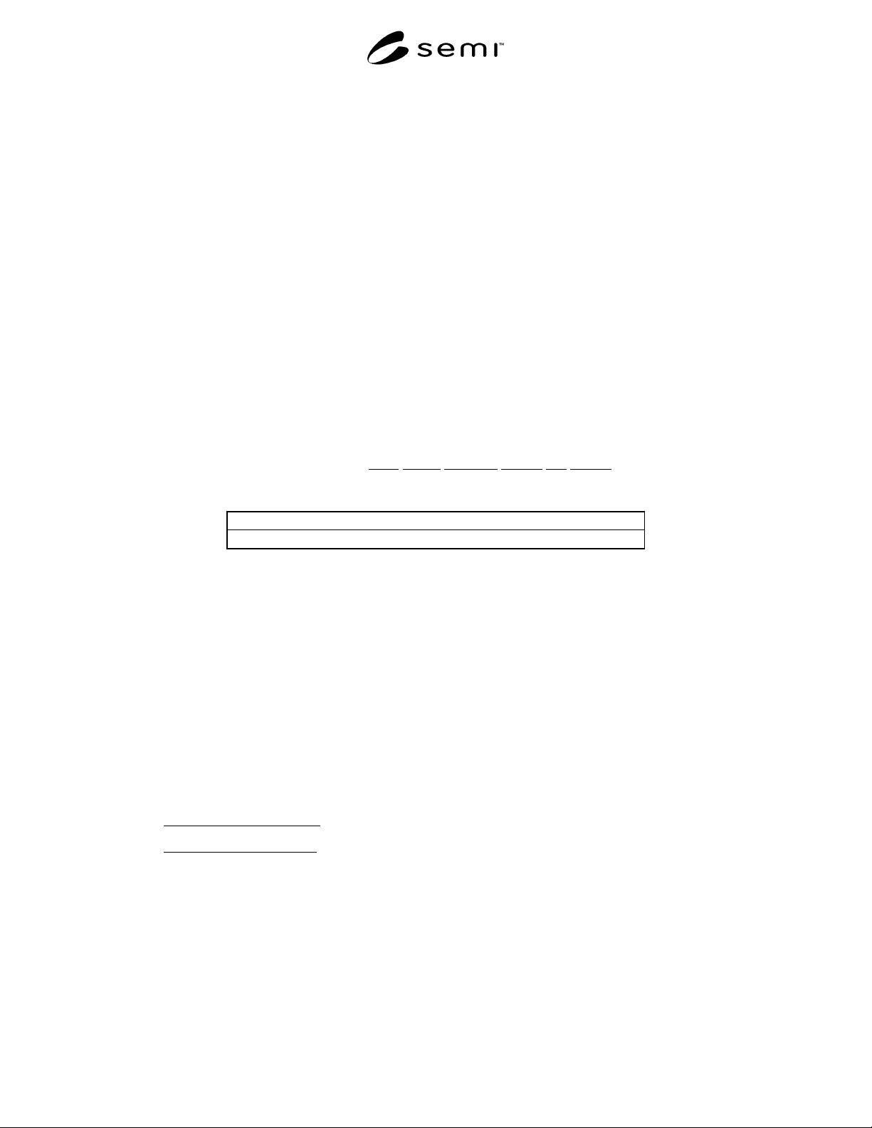
Normaliz ed (by lot) Die Offset (11) = Average Die Offset (3) - Average Lot Offset
(9) [Accuracy]
loti setj wafk diel
loti setj wafk diel
loti setj wafk diel loti setj wafk diel
xn
xoff
yn yoff
LOTX
LOTY
,, ,
,, ,
,, , ,, ,
=−
=−
(11)
A1-1.15.1 Discussion of Normalized (by lot) Die Offset
A1-1.15.1.1 This step is useful if you need to compare the variation between several different lots. It is not
completely necessary for the next step, since subtracting a constant from a string of numbers does not change the 3σ
variation, only the center point.
A1-1.16 Step 14 — Calculate
TTLX or TTLY = 3σ of Normalized (by lot) Die Offset (11) [Repeatability]
A1-1.16.1 Discussion fo TTLX or TTLY
A1-1.16.1.1 This is the value for determini ng (with 3σ confidence) whether your probe marks will always fall
within your desired spec. They are the hatch-marked lines.
A1-1.17 Step 15 — This normalized die offset includes Die-to-Die, Wafer-to-Wafer, and Setup-to-Setup offsets
thus a 3σ variation of this offset will be called Total Prober
Variation (TTLX and TTLY).
A1-1.17.1 Calculate Total Prober Error Range (3
σ
).
LOTX + TTLX, LOTX - TTLX = Total Prober X-Error Range (3σ)
LOTY + TTLY, LOTY - TTLY = Total Prober Y-Error Range (3σ)
A1-1.17.2 Suggested Graphs:
X-Offset Y-Offset
LOTX + TTLX LOTY + TTLY
LOTX LOTY
LOTX - TTLX LOTY - TTLY
Average Die X-Offset (3) Average Die Y-Offset (3)
A1-1.17.2.1
It is recommended to create on e graph illustrating the prober accuracy in X and one graph for Y.
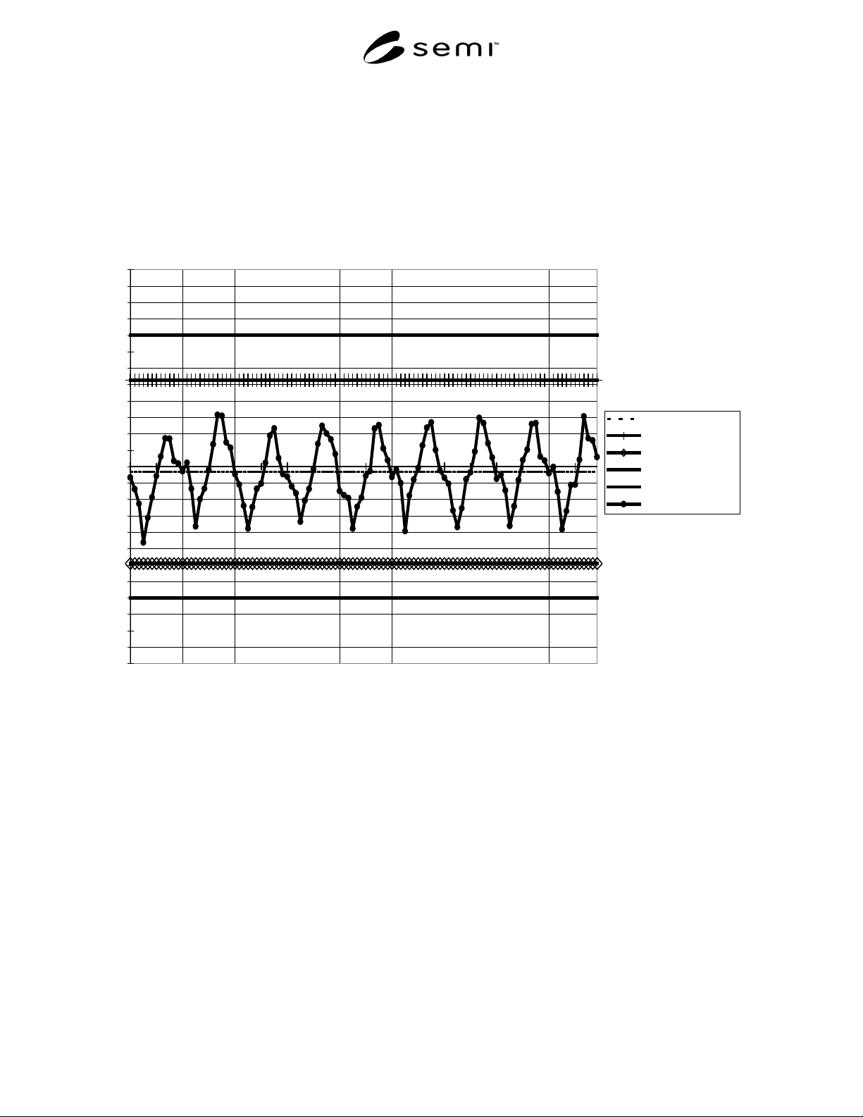
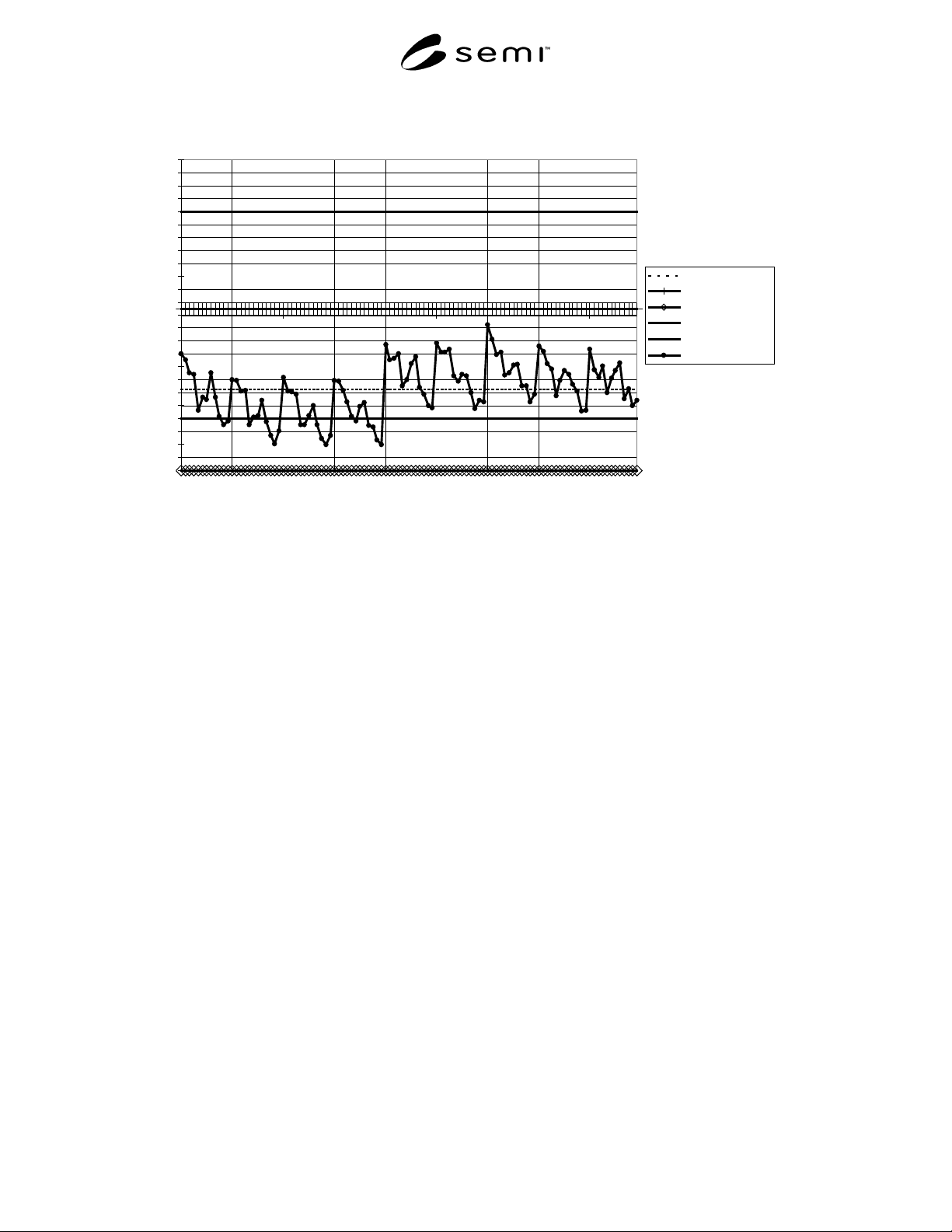
A1-1.18 Discussion of Graphs (one exa mple for X [Figure X] and one for Y [Figure Y])
A1-1.18.1 Average Lot X-Offset is the va lue from Step 10. This number shows where the probe mark distribution
is centered (the accuracy of the prober).
A1-1.18.2 Average Lot X-Offset +3σ is t he result from step 10 + the result from step 14
A1-1.18.3 Average Lot X-Offset -3σ is th e result from step 10 – the result from step 14
A1-1.18.4 These two lines show the ± 3σ range of your distribution. This describes the repeatability of the prober.
NOTE: There will always be explainable and unexplainable accuracy and repeatability errors on a prober. If these two lines fall
within your desired specification, you will probably not have any problems. The example graph for X-offset illustrates a well-
behaved, or “passing” prober. The example graph for Y-offset, on the other hand, is representative of a prober which failed to
meet the desired accuracy specification.
A1-1.18.5 The upper and lower desired specification limits have been added to the graphs.
A1-1.18.6 The final piece of data added t o the graph is the Average Die Offset. This, as stated in Step 1, is very
good at illustrating any trends throughout the lot.
SEMI G78-0699 © SEMI 199919
A1-1.18.7 Tips for graph making:
• Add gridlines across the X-axis to separate wafers.
• Print all graphs (X and Y, different lots, different probers) with the same scale in X and Y.
• Add a legend to your graphs, so that they will be readable by your “audience” as well as yourself.
Avg Lot X-Offset
Avg Lot X-Offset +3s
Avg Lot X-Offset -3s
Lower Spec Limit
Upper Spec Limit
Avg Die X-Offset
Figure 7
X-Offset
SEMI G78-0699 © SEMI 1999 20
Avg Lot Y-Offset
Avg Lot Y-Offset +3s
Avg Lot Y-Offset -3s
Lower Spec Limit
Upper Spec Limit
Average Die Y-Offset
Figure 8
Y-Offset
NOTICE: These standards do not purport to address
safety issues, if any, associated with their use. It is the
responsibility of the user of these standards to establish
appropriate safety and health practices and determine
the applicability of regulatory limitations prior to use.
SEMI makes no warranties or representations as to the
suitability of the standards set forth herein for any
particular application. The determination of the
suitability of the standard is solely the responsibility of
the user. Users are cautioned to refer to manufacturer’s
instructions, product labels, product data sheets, and
other relevant literature respecting any materials
mentioned herein. These standards are subject to
change without notice.
The user’s attention is called to the possibility that
compliance with this standard may require use of
copyrighted material or of an invention covered by
patent rights. By publication of this standard, SEMI
takes no position respecting the validity of any patent
rights or copyrights asserted in connection with any
item mentioned in this standard. Users of this standard
are expressly advised that determination of any such
patent rights or copyrights, and the risk of infringement
of such rights, are entirely their own responsibility.
Copyright by SEMI® (Semiconductor Equipment and Materials
International), 3081 Zanker Road, San Jose, CA 95134. Reproduction o
f
the contents in whole or in part is forbidden without express written
consent of SEMI.