semi合集-English.pdf - 第5034页
SEMI M18-0704 © SEMI 1990, 2004 20 26.3 Bonded Interface Location [ ] at SOI/BOX interf ace [ ] within BOX layer [ ] at BOX/Substrate in terface 100258 26.4 BOX Pinholes ≤ [ ] (/cm 2 ) 100259 T est Method [ ] Cu plating,…
SEMI M18-0704 © SEMI 1990, 2004 19
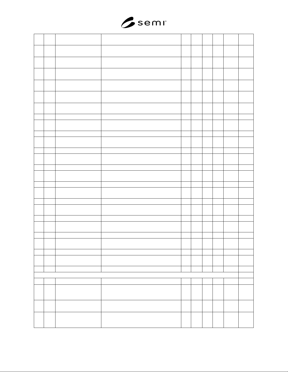
Roughness (Si surface)
rms @ 10 × 10µm
≤ [ ] (nm) 100243
Test Method
[ ] Atomic force microscope,
[ ] Others:
Roughness (Si surface)
rms@ [ ] × [ ]µm
≤ [ ] (nm) 100244
Test Method
[ ] Atomic force microscope,
[ ] Others:
Roughness (Si surface)
rms@ [ ] × [ ]µm
≤ [ ] (nm) 100245
Test Method
[ ] Atomic force microscope,
[ ] Others:
25.17 Surface Metal (Fe)
Contamination
≤ [ ] (/cm
2
) 100246
Test Method [ ] TXRF, [ ] AAS, [ ] ICP-MS
Surface Metal (Cr)
Contamination
≤ [ ] (/cm
2
) 100247
Test Method [ ] TXRF, [ ] AAS, [ ] ICP-MS
Surface Metal (Ni)
Contamination
≤ [ ] (/cm
2
) 100248
Test Method [ ] TXRF, [ ] AAS, [ ] ICP-MS
Surface Metal (Cu)
Contamination
≤ [ ] (/cm
2
) 100249
Test Method [ ] TXRF, [ ] AAS, [ ] ICP-MS
Surface Metal [ ]
Contamination
≤ [ ] (/cm
2
) 100250
Test Method [ ] TXRF, [ ] AAS, [ ] ICP-MS
Surface Metal [ ]
Contamination
≤ [ ] (/cm
2
) 100251
Test Method [ ] TXRF, [ ] AAS, [ ] ICP-MS
Surface Metal [ ]
Contamination
≤ [ ] (/cm
2
) 100252
Test Method [ ] TXRF, [ ] AAS, [ ] ICP-MS
Surface Metal [ ]
Contamination
≤ [ ] (/cm
2
) 100253
Test Method [ ] TXRF, [ ] AAS, [ ] ICP-MS
Surface Metal [ ]
Contamination
≤ [ ] (/cm
2
) 100254
Test Method [ ] TXRF, [ ] AAS, [ ] ICP-MS
Surface Metal [ ]
Contamination
≤ [ ] (/cm
2
) 100255
Test Method [ ] TXRF, [ ] AAS, [ ] ICP-MS
26. BOX CHARACTERISTICS
♦
26.1 BOX Thickness [ ] (nm) See NOTE 8 100256
Test Method [ ] Spectroscopic ellipsometry,
[ ] Spectroscopic reflectometry,
[ ] Others
♦
26.2 BOX Thickness Variation [ ] ≤ ± [ ] (nm),
[ ] ≤ ± [ ] (%)
100257
Test Method [ ] Spectroscopic ellipsometry,
[ ] Spectroscopic reflectometry,
[ ] Others:
SEMI M18-0704 © SEMI 1990, 2004 20
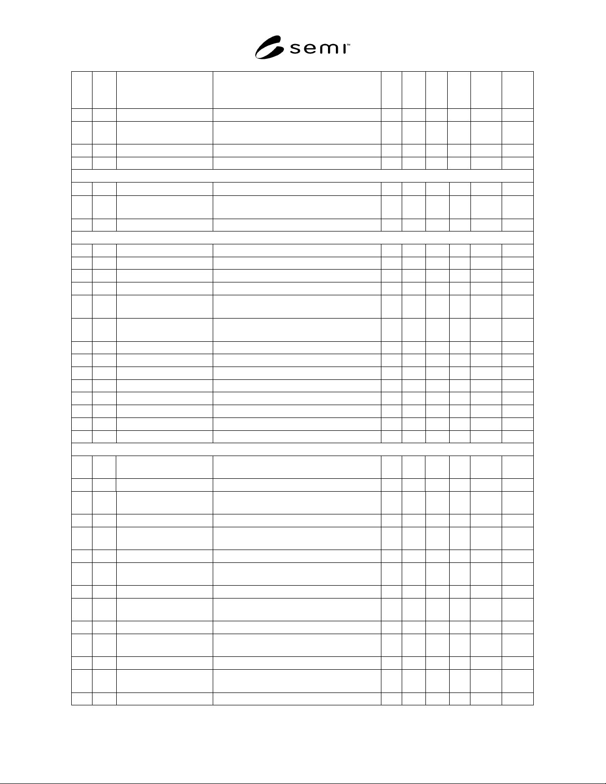
26.3 Bonded Interface
Location
[ ] at SOI/BOX interface
[ ] within BOX layer
[ ] at BOX/Substrate interface
100258
26.4 BOX Pinholes ≤ [ ] (/cm
2
) 100259
Test Method [ ] Cu plating,
[ ] BOX capacitor, [ ] Others:
26.5 Dielectric Breakdown > [ ] (MV/cm) 100260
Test Method [ ] BOX capacitor, [ ] Others:
27. MECHANICAL CHARACTERISTICS
27.1 Warp
≤ [ ] (µm)
100261
Test Method [ ] Automated noncontact scanning
[ ] Others:
27.2 Flatness-site See NOTE 8 100262
28. FRONT SURFACE INSPECTION CHARACTERISTICS
28.1 Scratch None 100263
Test Method [ ] Visual, [ ] Others:
28.2 Haze None 100264
Test Method [ ] Visual, [ ] Others:
28.3 LLS
@particle size
≤ [ ] (/cm
2
)
@ ≥ [ ] (µm)
100265
100266
Test Method [ ] Automated particle counter
[ ] Others:
28.4 Slip See NOTE 8 100267
Test Method [ ] Visual, [ ] Others:
28.5 Edge Chip [ ]SEMI M1, [ ]Others: 100268
Test Method [ ] Visual, [ ] Others:
28.6 Edge Crack [ ]SEMI M1, [ ]Others: 100269
Test Method [ ] Visual, [ ] Others:
28.7 Foreign Matter See NOTE 8 100270
Test Method [ ] Visual, [ ] Others:
29. BACK SURFACE CHARACTERISTICS
29.1 Backside Metal (Fe)
Contamination
≤ [ ] (/cm
2
) for each atom 100271
Test Method [ ] TXRF, [ ] AAS, [ ] ICP-MS
Backside Metal (Cr)
Contamination
≤ [ ] (/cm
2
) 100272
Test Method [ ] TXRF, [ ] AAS, [ ] ICP-MS
Backside Metal (Ni)
Contamination
≤ [ ] (/cm
2
) 100273
Test Method [ ] TXRF, [ ] AAS, [ ] ICP-MS
Backside Metal (Cu)
Contamination
≤ [ ] (/cm
2
) 100274
Test Method [ ] TXRF, [ ] AAS, [ ] ICP-MS
Backside Metal [ ]
Contamination
≤ [ ] (/cm
2
) 100275
Test Method [ ] TXRF, [ ] AAS, [ ] ICP-MS
Backside Metal [ ]
Contamination
≤ [ ] (/cm
2
) 100276
Test Method [ ] TXRF, [ ] AAS, [ ] ICP-MS
Backside Metal [ ]
Contamination
≤ [ ] (/cm
2
) 100277
Test Method [ ] TXRF, [ ] AAS, [ ] ICP-MS
SEMI M18-0704 © SEMI 1990, 2004 21
Backside Metal [ ]
Contamination
≤ [ ] (/cm
2
) 100278
Test Method [ ] TXRF, [ ] AAS, [ ] ICP-MS
Backside Metal [ ]
Contamination
≤ [ ] (/cm
2
) 100279
Test Method [ ] TXRF, [ ] AAS, [ ] ICP-MS
Backside Metal [ ]
Contamination
≤ [ ] (/cm
2
) 100280
Test Method [ ] TXRF, [ ] AAS, [ ] ICP-MS
1. Individual value is not required if wafer is specified according to SEMI M1. _____.
2. Flatness Acronyms are determined from the Flatness Decision Tree in SEMI M1, Appendix 1.
3. Individual value is not required if wafer is specified according to SEMI M1, Table 1.
4. Individual value is not required if wafer is specified according to Table 1 of SEMI M2 or SEMI M11.
5. Haze, Teracing, Surface micro-roughness, Nanotopography, and other attributes may be discussed between supplier and user.
6. Support-related backside defects may be discussed between supplier and user
7. Surface boron depletion, dissolved hydrogen in the case of hydrogen annealed wafer, Post-annealed oxygen, and Silicon nitride precipitates
and defects in the case of nitrogen-doped silicon may be discussed between supplier and user.
8. To be specified or discussed between users and suppliers.
9. Thinner SOI is to be discussed between users and suppliers.
10. It is specified by a distance from the FQA boundary to the periphery of a base wafer of nominal dimensions. It is not a distance from an edge
of an SOI layer.
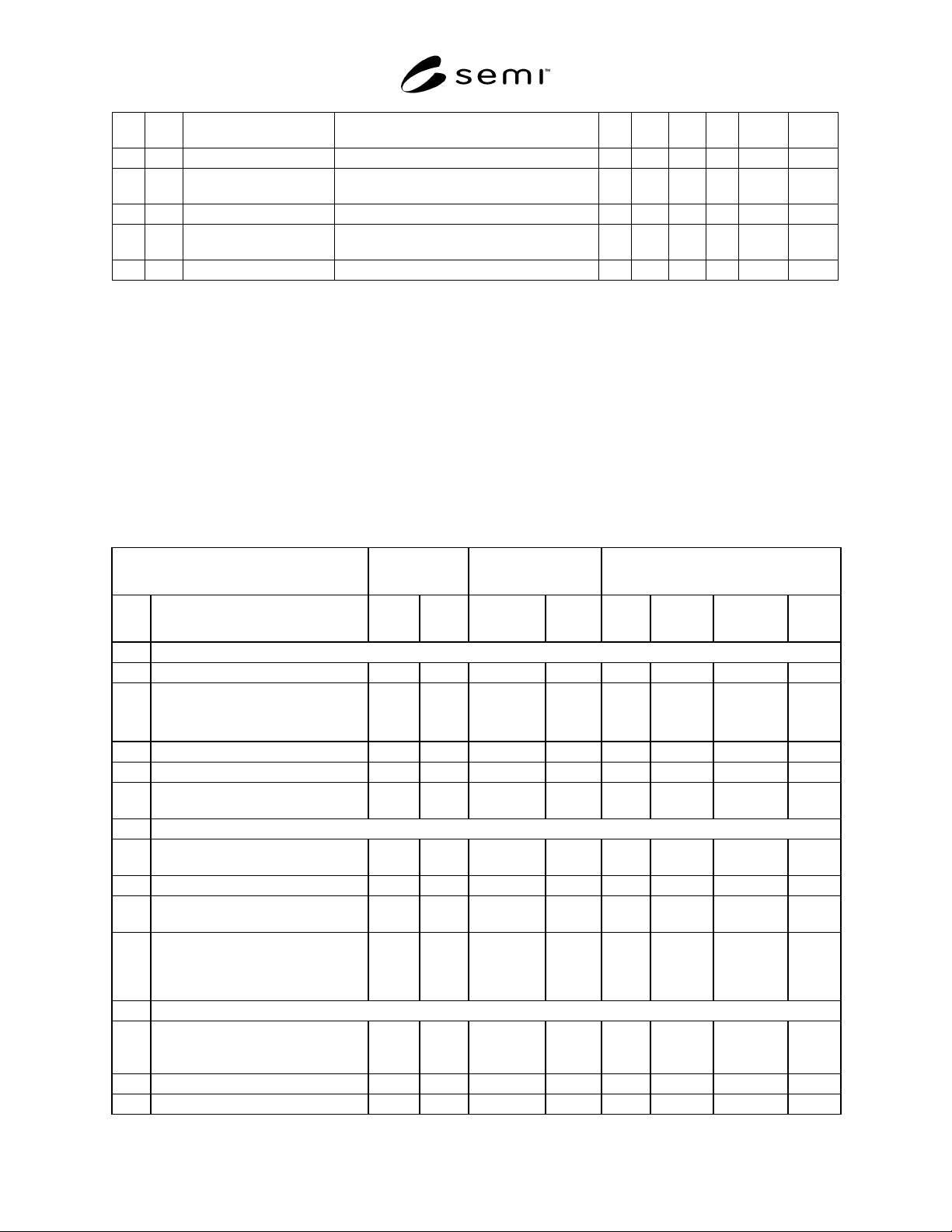
Table 1 Industry Standard References
Polished Wafer
ITEM VALUE STANDARD
REFERENCE
A
STANDARD TEST METHODS
IS IN
SEMI
IS
REQ'D
B
SEMI JEIDA ASTM SEMI JIS JEIDA DIN
1. GENERAL CHARACTERISTICS
1.1 Growth Method NO YES M1 Note 5 MF26
1.2 Crystal Orientation NO YES MF42 18 50433/1
50433/2
50433/3
1.3 Conductivity Type NO YES M1 Note 5 H 607 50432
1.4 Dopant NO YES M1 Note 5 50438/3
1.5 Nominal Edge Exclusion Distance for
Fixed Quality Area
NO NO M1 Fig 1
2. ELECTRICAL CHARACTERISTICS
2.1 Resistivity NO YES M1 Sec 9 MF84,
MF673
H 602 18
H 612
50431,
50447
2.2 Radial Resistivity Variation (RRG) NO NO M1 Sec 9 MF81 18 50435
2.3 Resistivity Striations NO NO MF154,
MF525
2.4 Minority Carrier Lifetime NO NO MF28,
MF391,
MF1388,
FM1535
H 604 53 50440
3. CHEMICAL CHARACTERISTICS
3.1 Oxygen Concentration NO NO MF1188,
MF1366,
MF1619
61 50438/1
3.2 Radial Oxygen Variation NO NO MF951
3.3 Carbon Concentration NO NO MF1391 56 50438/2