semi合集-English.pdf - 第6164页
SEMI G34-89 © SEMI 198 6, 1996 4 Seal Ar ea Figure 5 Seal Area NOTICE: T hese standards do not purport to ad dress safety issues, if any, ass o ciated with their use. It is the responsibilit y of the user of these sta nd…
SEMI G34-89 © SEMI 1986, 19963
9.5 Solderability — Per MIL-STD-883, Method 2003.
9.6 Sequence of Events and Incoming Testing —
During incoming inspection, the sequence of testing
shall be:
1. Frame Attach
2. Die Attach
3. Bond (if applicable)
4. Seal
5. Lead Finish (Type A per MIL-M-38510)
6. Environmental Testing
7. Lead Trim
8. Fine Leak
9. Gross Leak
10. Torque Test (test method pending)
11. Bond Pull
12. Die Shear (optional)
9.6.1 Solderability — A separate sample with lead
finish Type A shall be subjected to preconditioning of
Class B time/temperature exposure per burn-in Test
Method 1015, MIL-STD-883, then tested to Method
2003.
NOTE: An initial qualification on the thermal and electrical
characteristics of the package may be performed. The
characteristics tested will be:
Insulation Resistance — Per MIL-STD-883, Method
1003, Test Condition B.
Thermal Dissipation — Per MIL-STD-883, Method
1012.
10 Packaging and Marking
10.1 Packaging — Containers selec ted shall be strong
enough and suitably designed to provide maximum
protection against crushing, spillage, and other forms of
damage to the container or its contents. Containers shall
afford protection of the contents from contamination
and exposure to excessive moisture or oxidation by
gases. Packaging materials shall be so selected to
prevent any contamination of the ceramic component
parts with paper fibers or organic particles.
10.2 Marking — The outer containers shall be clearly
marked to identify the user stock number, user purchase
order number, drawing number, quantity, vendor lot
number, and solder glass type.
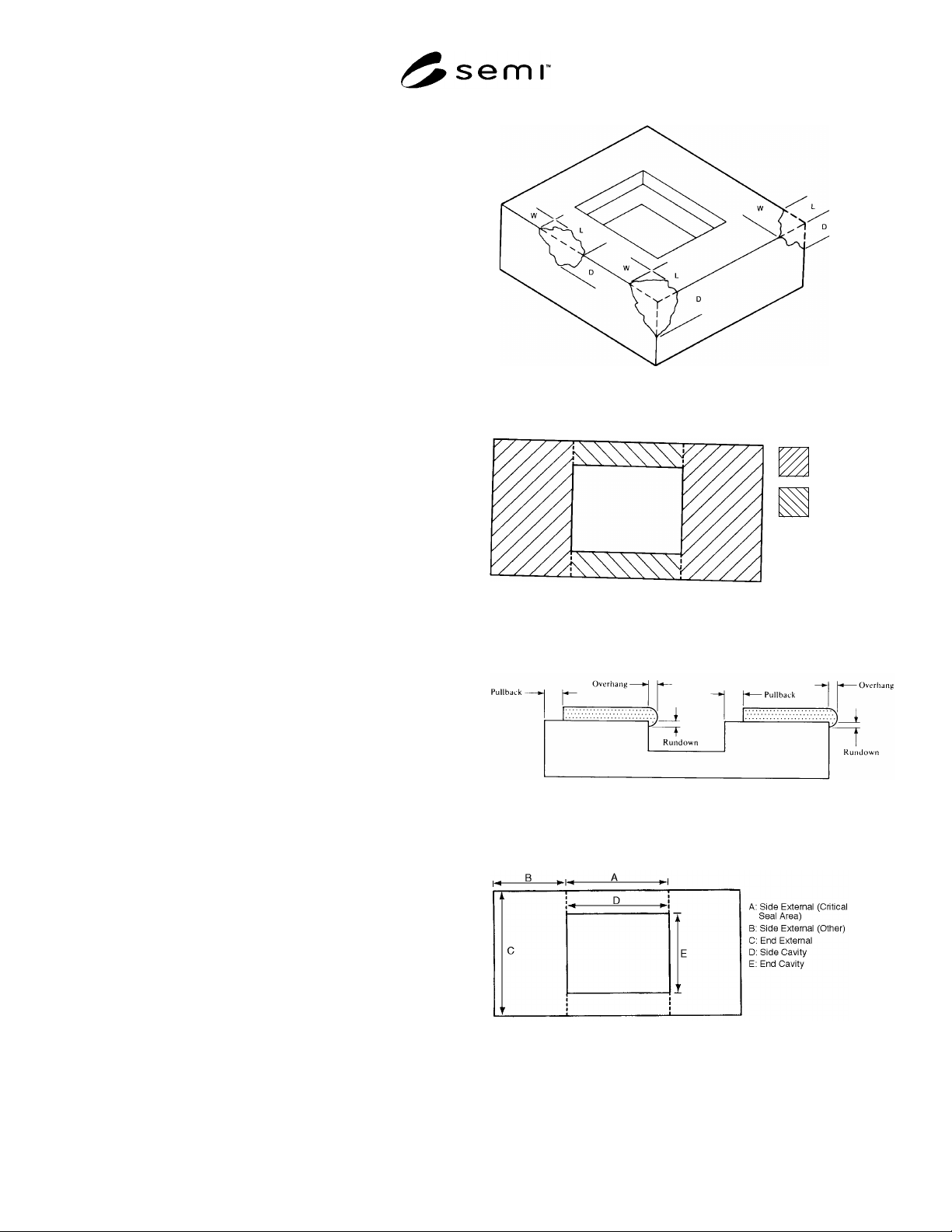
Figure 1
Chip Illustration
Non-Critical
Critical
Figure 2
Critical and Non-Critical Seal Areas
Figure 3
Glass Misalignment
Figure 4
Pullback Measurement Area
SEMI G34-89 © SEMI 1986, 1996 4
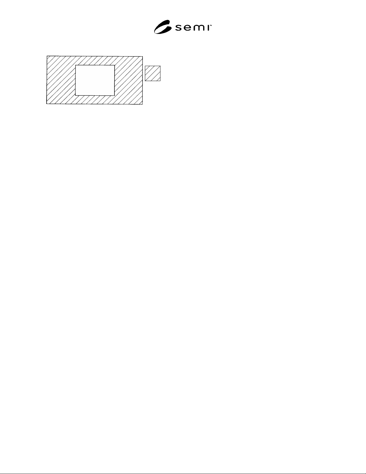
Seal Area
Figure 5
Seal Area
NOTICE: These standards do not purport to address
safety issues, if any, associated with their use. It is the
responsibility of the user of these standards to establish
appropriate safety and health practices and determine
the applicability of regulatory limitations prior to use.
SEMI makes no warranties or representations as to the
suitability of the standards set forth herein for any
particular application. The determination of the
suitability of the standard is solely the responsibility of
the user. Users are cautioned to refer to manufacturer’s
instructions, product labels, product data sheets, and
other relevant literature respecting any materials
mentioned herein. These standards are subject to
change without notice.
The user’s attention is called to the possibility that
compliance with this standard may require use of
copyrighted material or of an invention covered by
patent rights. By publication of this standard, SEMI
takes no position respecting the validity of any patent
rights or copyrights asserted in connection with any
item mentioned in this standard. Users of this standard
are expressly advised that determination of any such
patent rights or copyrights, and the risk of infringement
of such rights, are entirely their own responsibility.
Copyright by SEMI® (Semiconductor Equipment and Materials
International), 3081 Zanker Road, San Jose, CA 95134. Reproduction of
the contents in whole or in part is forbidden without express written
consent of SEMI.

SEMI G35-87 © SEMI 1986, 19871
SEMI G35-87
SPECIFICATION FOR TEST METHODS FOR LEAD FINISHES ON
SEMICONDUCTOR (ACTIVE) DEVICES
1 Scope
This specification shall be used by suppliers and/or
users of semiconductor (active) devices, and is effective
for all lead finishes used.
2 Purpose
This specification establishes uniform methods and
procedures for conducting tests on lead finishes on
(active device) electronic packages. Other SEMI
standards establish materials used and the finishes for
them.
3 Applicable Documents
3.1 Order of Precedence — In the event of a conflict
between the text of this specification and the references
cited herein, the text of this specification shall take
precedence.
3.2 Referenced Documents — Unless otherwise
specified, the following standards and specifications,
with appropriate issue letter at time of order entry, form
a part of this specification to the extent and for the
purpose specified herein.
3.3 ASTM Specifications
1
E 10 — Standard Test Method for Brinell Hardness for
Metallic Materials
E 122 — Choice of Sample Size to Estimate the
Average Quality of a Lot or Process
E 384 — Standard Test Methods for Micro-Hardness of
Materials
B 487 — Measuring Metal and Oxide Coating
Thickness by Microscopical Examination of a Cross
Section
B 545 — Standard Specification for Electro Deposited
Coatings of Tin
B 567 — Measurement of Coating Thickness by the
Beta Backscatter Principle
B 568 — Measurement of Coating Thickness by X-Ray
Spectrometry
3.4 Military Specifications
2
1 American Society for Testing and Materials, 100 Barr Harbor
Drive, West Conshohoken, PA 19428-2959
MIL-STD-883 — Test Methods and Procedures for
Microelectronics
MIL-STD-105 — Sampling Procedures with Tables for
Inspection by Attributes
3.5 SEMI Specifications
SEMI G4 — Integrated Circuit Leadframe Materials
Used in the Production of Stamped Leadframes
SEMI G18 — Integrated Circuit Leadframe Materials
Used in the Production of Etched Leadframes
SEMI G20 — Lead Finishes for Plastic Packages
(Active Devices Only)
4 Selected Definitions
active devices — semiconductor devices with active
function (e.g., IC, transistor, diode) as opposed to
passive devices (e.g., inductors, capacitors).
air atmosphere — air heated to specified temperature
which, when cooled to ambient, will normalize to one
(1) standard atmosphere.
steam atmosphere — atmosphere in a closed vessel
containing water, with venting sufficient to maintain
temperature at one (1) standard atmosphere and 100° +
0, -5°C.
NOTE: The intent of this requirement is to replace air with
steam.
5 Sampling
Unless otherwise specified, Practice E 122 shall be
used. When so specified, appropriate sample sizes shall
be selected from each lot in accordance with MIL-STD-
105. Each quality characteristic shall be assigned an
acceptable quality level (AQL) and lot tolerance
percent defective (LTPD) value in accordance with
MIL-STD-105 definitions for critical, major, and minor
classifications. If desired and so specified in the
contract or order, each of these classifications may
alternatively be assigned cumulative AQL and LTPD
values. Inspection levels shall be agreed upon between
the user and supplier.
2 Military Standards, Naval Publications and Form Center, 5801
Tabor Avenue, Philadelphia, PA 19120