semi合集-English.pdf - 第7345页
SEMI MF1390-1104 © SEMI 2004 5 NOTE 5: From Figure 1, note that th e distance between Probe A and the nearest surface of the wafer is displac ement value a and the distance between Probe B and the nearest surface of the …

SEMI MF1390-1104 © SEMI 2004 4
between the warp value obtained by the measuring
equipment under test and the reference warp value (see
Section 9).
8.3 Representative Wafer — required only if the
Representative Wafer Inversion Method is used for the
gravity correction. A representative wafer shall be
identical in nominal diameter, nominal thickness,
fiducials, composition and crystalline orientation to
those being measured. Its warp need not be known.
9 Suitability of Measuring Equipment
9.1 Determine the suitability of the measuring
equipment with the use of a reference wafer and its
reference warp value in accordance with the
procedures of Sub-section 9.2, or by performance of a
statistically-based instrument repeatability study to
ascertain whether the equipment is operating within the
manufacturer's stated specification for repeatability.
9.1.1 The reference warp value is the average of a
number of values obtained for that wafer over a number
of “passes” (repeat measurements). The reference
wafer is measured on the measuring equipment under
test and its reference warp value is compared against
the measured warp value. The acceptable level of the
agreement between the reference and measured warp
values is to be agreed upon by the parties to the test.
9.2 Procedure
9.2.1 Select a reference wafer of appropriate criteria,
together with its associated reference warp value.
9.2.2 Measure the reference wafer on the measuring
equipment under test to obtain a sample warp value.
9.2.3 Subtract the two warp values to obtain the
difference:
samplereferencewarp
WarpWarp
(1)
9.2.4 The metric to be used to determine acceptability
is difference,
warp.
Accept the measuring equipment as
suitable for use if this difference is less than a value that
is agreed upon between the parties to the test.
NOTE 4: If the measuring equipment is to be used to
measure other parameters, such as flatness and thickness
variation in addition to warp, the reference and sample warp
values may be included in the reference and sample data sets
specified in SEMI MF1530, but this is not necessary if only
warp measurements are to be made.
10 Sampling
10.1 This test method is nondestructive and may be
used on either 100% of the wafers in a lot or on a
sampling basis.
10.1.1 If samples are to be taken, procedures for
selecting the sample from each lot of wafers to be tested
shall be agreed upon between the parties to the test, as
shall the definition of what constitutes a lot.
11 Calibration and Standardization
11.1 Calibrate the measuring equipment in accordance
with the manufacturer's instructions.
11.2 When using the Representative Wafer Inversion
Method for correcting the gravity-induced deflection,
determine z
gravity
, the deflection due to gravity and
machine effects on the representative wafer, in
accordance with Section 12 and Section 13 through
paragraph 13.7.
12 Procedure
12.1 Prepare the apparatus for measurement of wafers,
including selection of diameter, peripheral fiducials,
scan area and data display/output functions. Also select
the gravitational correction method from one of the
following:
Reference Wafer Inversion Method (see Note 3),
Sample Wafer Inversion Method, or
Theoretical Modeling Method.
12.2 Select the fixed quality area (FQA) by specifying
the nominal edge exclusion (EE).
12.3 Introduce the test specimen into the measurement
mechanism with the front surface upward and initiate
the measurement sequence to determine and record the
distances between each probe and the nearest wafer
surface in pairs, a and b, at each measurement position.
Proceed directly to Section 13 unless (1) the Sample
Wafer Inversion Method is being used to correct for
effects of distortion due to gravity or (2) a
representative wafer is being measured to obtain the
gravity correction for use in the Representative Wafer
Inversion Method (see Note 3).
12.4 Repeat Section 12.2 with the wafer inverted (front
surface downward).
13 Calculations
13.1 The following calculations are performed
automatically within the instrument. An outline of the
calculation structures is provided here to indicate the
nature of the procedure.
13.2 Determine the displacements (distances) between
each probe and the nearest surface of the wafer (in
pairs) at intervals along the scan pattern.

SEMI MF1390-1104 © SEMI 2004 5
NOTE 5: From Figure 1, note that the distance between
Probe A and the nearest surface of the wafer is displacement
value a and the distance between Probe B and the nearest
surface of the wafer is displacement value b.
13.3 Set the origin of the z-axis at the midpoint between
the two probes, A and B.
13.4 Find the distance, z
m
, of the median surface from
the z-axis origin at each point. From Figure 1,
22
t
a
D
z
m
(2)
and
22
t
b
D
z
m
(3)
Therefore,
m
z
t
b
Dt
a
D
2
2222
(4)
and
2
ab
z
m
(5)
where
D = distance between Probes A and B,
a = distance between Probe A and the nearest
(top) wafer surface,
b = distance between Probe B and the nearest
(bottom) wafer surface, and
t = wafer thickness.
13.5 For measurements in the normal orientation (front
surface up), call the position of the median surface z
nor
.
13.6 For measurements in the inverse orientation (back
surface up), call the position of the median surface z
inv
.
13.7 For measurements on representative wafers or on
sample wafers when the Sample Wafer Inversion
Method is being used, determine the gravitational
correction to the median surface as follows:
2
invnor
gravity
zz
z
(6)
NOTE 6: This cancels the effect of the representative wafer's
shape while retaining the effect of gravity.
13.8 Determine the gravity compensated median sur-
face as follows:
13.8.1 Representative Wafer Inversion Method —
Subtract z
gravity
from z
nor
to produce z
com
at each
measurement point.
NOTE 7: The Representative Wafer Inversion Method deals
not only with first-order gravitational effects, but also with
other effects that may influence the measured value, such as
wafer-periphery effects, some machine-specific signature, etc.
13.8.2 Sample Wafer Inversion Method — Subtract
z
gravity
from z
nor
to produce z
com
at each measurement
point. Note that this is equivalent to taking the
difference between the normal and inverted
measurement values at each point:
22
invnorinvnor
norgravitynorcom
zzzz
zzzz
(7)
13.8.3 Theoretical Modeling Method — Apply
gravitational correction developed from a theoretical
model. Although a rigorous model is not known to
exist, approximate corrections have been calculated
3
(see Related Information 1).
13.9 Construct a reference plane that is a least-squares
fit to the gravity-compensated median surface data at all
the points of the of the scan pattern. The reference
plane is of the form:
RRRref
cybxaz
(8)
where a
R
, b
R
, and c
R
are constants selected so that
yx
RRRcom
cybxayxz
,
2
)](),([ (9)
is minimized over the FQA (see Section 12.2).
13.10 Subtract the z-value of the reference plane (z
ref
)
from the compensated z-value, z
com
, at all the points of
the scan pattern to yield the reference plane deviation
(RPD) at each point:
refcom
zzRPD
(10)
13.11 Calculate the warp of the wafer as the difference
between the maximum (most positive) and minimum
(most negative) RPD:
minmax
warp RPDRPD
(11)
13.12 Record the calculated warp value.
13.13 For referee or other measurements where the
wafer is measured more than once, calculate the
maximum, minimum, sample standard deviation,
average, and range of all measurements on the sample.
3 Application Note: “Gravitational Sag in Silicon Wafers,” ADE
Corporation, 80 Wilson Way, Westwood, MA 02090-1806, Nov. 20,
1991.
SEMI MF1390-1104 © SEMI 2004 6
13.13.1 Record sample standard deviation and other
statistical parameters as agreed upon between the
parties to the test.
14 Report
14.1 Report the following information:
14.1.1 Date, time, and temperature of test,
14.1.2 Identification of operator,
14.1.3 Location (laboratory) of test,
14.1.4 Identification of measuring instruments, inclu-
ding wafer-holding device diameter, data point spacing,
sensor size, and gravitation-correction method,
14.1.5 Lot identification, including nominal diameter,
nominal center-point thickness, and nominal edge
exclusion (EE) specified.
14.1.6 Description of sampling plan, if any, and
14.1.7 Warp of each wafer measured.
14.2 For referee tests also include in the report the
standard deviation of each set of wafer measurements
and such other statistical parameters as have been
agreed to by the parties to the test.
15 Precision
15.1 Twenty-three 200 mm diameter, single-side
polished silicon wafers were employed in a round-robin
experiment. These wafers represented three different
manufacturing processes. All three subsets were bare
on the front surface. Two subsets were bare on the
back surface and one subset had oxide on the back
surface.
15.2 Eight laboratories measured warp. Warp value
ranges for these three subsets are shown in Table 1.
Each of the twenty-three wafers was measured three
times in succession (in three cassette-to-cassette
“passes”), on a single day on automatic measurement
systems in accordance with this test method.
15.3 All measurement data were acquired with 3 mm
nominal edge exclusion.
15.4 The number of laboratories, samples, and
determinations in this study met the minimum
requirements for determining precision prescribed in
ASTM Practice E 691.
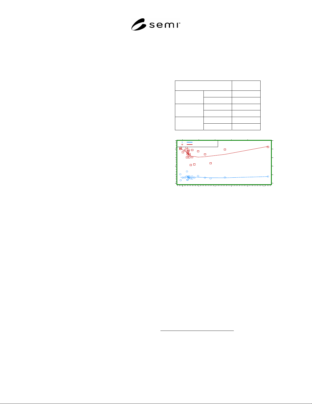
15.5 The ranges of 95% confidence interval, within
which two measurements are considered statistically to
be the same, for within-laboratory repeatability (r) and
between-laboratory reproducibility (R) are shown in
Table 1.
15.6 Figure 2 contains plots of the 95% confidence
intervals for repeatability (r) and reproducibility (R)
against mean value of warp.
15.7 For more details, refer to the Research Report.
4
Table 1 Summary Warp Measurement Statistics
Parameter Warp
Smallest 4.30
Mean, m
Largest 31.25
Smallest 0.184
r, m
Largest 0.695
Smallest 1.112
R, m
Largest 2.097
Figure 2
Warp Repeatability & Reproducibility
16 Bias
16.1 Bias — No standards exist against which the bias
of this test method can be evaluated.
17 Keywords
non-contact measurement; semiconductor; shape;
silicon; wafers; warp
4 Available on request from SEMI Headquarters, Publications
Department, San Jose, CA, Fax: 408-943-7015. Request International
Standards Research Report F01-1016, ASTM Interlaboratory Round
Robin Experiment on Measuring Warp on Silicon Wafers by
Automated Noncontact Scanning and Measuring Flatness, Thickness
and Thickness Variation of Silicon Wafers by Automated Noncontact
Scanning.
Mean Warp,
m
r and R, m
D
V
N
O
C
A
W
R
T
J
L
H
F
K
Q
E
G
M
S
I
U
P
B
D
V
N
O
C
A
W
R
T
J
L
H
F
K
Q
E
G
M
S
I
U
P
B
5 1015202530
0.0
0.5
1.0
1.5
2.0
2.5
Repeatability
Reproducibility