semi合集-English.pdf - 第5259页
SEMI M41-1101 © SE MI 2000, 2001 16 9.3.2 Test method — MOS h i gh-freque ncy C-V measurem e nt of a Box capacitor norm ally yields a flat band voltage. Details of the test structure and the test method are determined by…
SEMI M41-1101 © SEMI2000, 200115
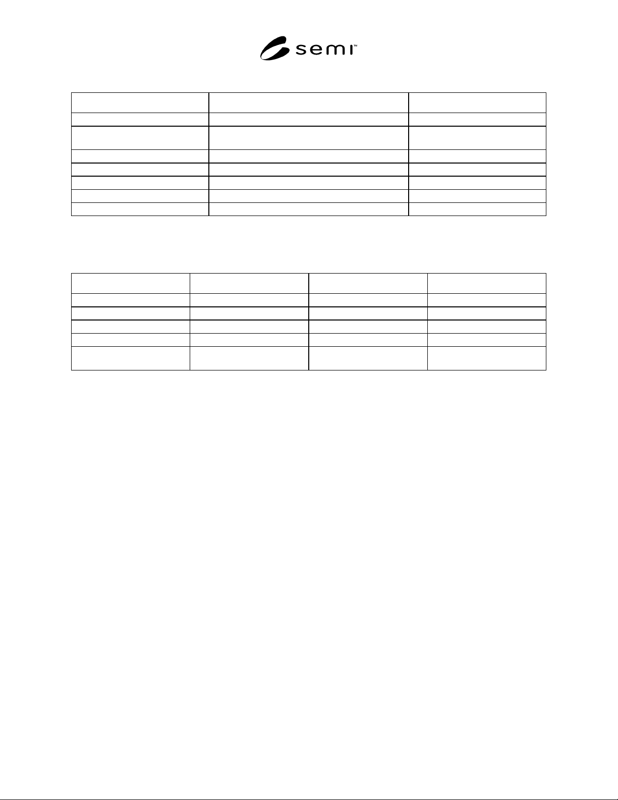
Table 7 Example: Soi Wafer Surface Visual Inspection Criteria
Criterion Items Allowed Quantity ( Per 150 mm Wafer ) Description
Haze NONE
Slip < 4
2 mm width and < 15 mm length
Scratches NONE
Chips / Cracks < 3 for @ 0.5 mm circumferential x 0.3 mm length Edge : Base Wafer
Pits and Dimples NONE
Particle Density ( LPD ) < 30 for @ > 0.2 µm <0.17 / cm
2
for 150 mm Wafer
Contamination NONE Both Surface and Backside
NOTE 1: The surface visual inspection is conducted under the collimated bright light.
NOTE 2: Non-SOI edge area (E.E. ) of 6 mm is applied to the criterion items except for edge chips/cracks.
NOTE 3: The whole wafer (Top silicon film and Base wafer) is inspected except for edge chips/cracks.
Table 8 Soi Electrical Parameters
Parameters Reference Value Method
Photo-conductivity Lifetime Section 9.1 To be determined µ-PCD
BOX Breakdown Section 9.2 To be determined I-V
BOX Charge Section 9.3 To be determined C-V
BOX Surface States Section 9.4 To be determined C-V
Doping Density
Top silicon film, Base wafer
Section 9.5 To be determined SIMS or 4 pt. probe
9 Electrical Parameters
9.1 Photo-conductivity Lifetime
9.1.1 Test Method:
µ-PCD method
9.1.1.1 Excess carriers that are created in the wafer by a light pulse increases the conductivity of the sample. When
the light is turned off, the conductivity is decreased by the carrier recombination. This phenom-enon is monitored
by means of microwave reflectance. The microwave detects an exponential decay in conduc-tivity, from which a
decay constant is determined.
9.1.2 The effective recombination lifetime τ
eff
is given by the following expression:
1/τ
eff
= 1/τ
B
+ 1/(τ
S
+ τ
D
)
τ
S
= d/(S
Si/Box
+ S
Si
), τ
D
= d/π
2
D
Where τ
B
is bulk recombination lifetime, τ
S
is surface recombination lifetime, τ
D
is diffusion lifetime, S
Si/Box
is
recombination velocity at the Box interface, S
Si
is recombination velocity at the silicon surface, D is diffusion
coefficient and d is top silicon film thickness.
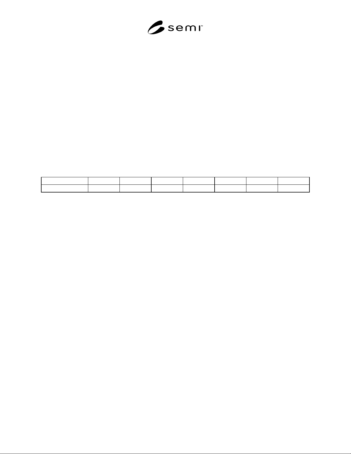
9.1.3 The wavelength of the light has to be selected, depending on the top silicon film thickness (see Table 9).
9.2 Box Breakdown Voltage
9.2.1 Test Structure –– Box capacitor having an area (Ex. 1 cm
2
).
9.2.2 Test Method: Staircase I-V Measurement –– Voltage is stepwise increased in one-volt increments from zero to
the (+/-) specified voltage. Details of the test structure and the test method are determined by negotiation between
wafer users and wafer suppliers.
9.3 Box Charge
9.3.1 Test Structure — Box capacitor having an area (Ex. 1 cm
2
).
SEMI M41-1101 © SEMI 2000, 2001 16
9.3.2 Test method — MOS high-frequency C-V measurement of a Box capacitor normally yields a flat band
voltage. Details of the test structure and the test method are determined by negotiation between wafer users and
wafer suppliers.
9.4 Buried Oxide Fast Interfaces State Density
9.4.1 Test Structure — Box capacitor having an area. (Ex. 1 cm
2
)
9.4.2 Test Method — High-Low Frequency MOS C-V.
9.4.3 If care is taken in their fabrication to minimize oxide surface damage and contamination during silicon
etching, good quality quasi-static MOS C-V curves can be measured. From comparison of high and low frequency
C-V curves, midgap interface state density can be determined. Details of the test structure and the test method are
determined by negotiation between wafer users and wafer suppliers.
9.5 Doping Density
9.5.1 Test Method — SIMS
9.5.1.1 Be careful of electrical charging up of test pieces due to the existence of BOX, the difference of detecting
sensitivity between silicon and silicon dioxide, and the existence of disturbance ions such as Si
30
H
1
in case of P
31
measurement.
Table 9 Relationship Between Wavelength of the Light and Penetration Depth
Wavelength [nm] 450 532 635 670 780 820 850
Depth [µm] ~ 0.8 ~ 1.4 ~ 3.0 ~ 4.0 ~ 10.0 ~ 14.0 ~ 18.0
9.5.2 Test Method — Four point probe
9.5.2.1 By contacting the equally spaced four point probes with a wafer and by supplying current between the outer
two probes, the voltage difference between the inner two probes is measured. The silicon resistivity ρ is determined
by the following equation (JIS H0602):
ρ= πV/ln2•I•d[Ωcm] if probe interval >> top silicon film thickness: d
9.5.3 The specific test method should be determined between wafer users and wafer suppliers.
10 Packing and Marking
10.1 Special packing requirements shall be subject to agreement between the users and the suppliers. Otherwise all
wafers shall be handled, inspected, and packed in such a manner as to avoid chipping, scratches and contamination,
and in accordance with the best industry practices to provide sample protection against damage during shipment.
10.2 The wafer supplied under these specifications shall be identified by appropriately labeling on the outside of
each box or other container and each subdivision thereof in which it may be reasonably expected that the wafers will
be stored prior to further processing. Identification marks, codes, symbols and content shall be agreed upon between
users and suppliers.
NOTICE: SEMI makes no warranties or representations as to the suitability of the standard set forth herein for any
particular application. The determination of the suitability of the standard is solely the responsibility of the user.
Users are cautioned to refer to manufacturer’s instructions, product labels, product data sheets, and other relevant
literature respecting any materials mentioned herein. These standards are subject to change without notice.
The user’s attention is called to the possibility that compliance with this standard may require use of copyrighted
material or of an invention covered by patent rights. By publication of this standard, SEMI takes no position
respecting the validity of any patent rights or copyrights asserted in connection with any item mentioned in this
standard. Users of this standard are expressly advised that determination of any such patent rights or copyrights, and
the risk of infringement of such rights, are entirely their own responsibility.
Copyright by SEMI® (Semiconductor Equipment and Materials
International), 3081 Zanker Road, San Jose, CA 95134. Reproduction o
f
the contents in whole or in part is forbidden without express written
consent of SEMI.

SEMI M42-1000 © SEMI 20001
SEMI M42-1000
SPECIFICATION FOR COMPOUND SEMICONDUCTOR EPITAXIAL
WAFERS
This specification was technically approved by the Global Compound Semiconductor Committee and is the
direct responsibility of the North American Compound Semiconductor Committee. Current edition approved
by the North American Regional Standards Committee on August 28, 2000. Initially available at
www.semi.org September 2000; to be published October 2000.
1 Purpose
1.1 Compound semiconductor epitaxial layers have
been extensively used for many years as the basis of
high speed electronics and optoelectronic devices.
There are suppliers of epitaxial layers who will grow
material to the customer’s specification. There is a
need to define standardized descriptive terms, tolerance
schedules and recommended test methods to reduce
ambiguity in the interpretation of specifications for
such wafers. Special emphasis is placed on the
definitions pertaining to uniformity. This proposed
document addresses only the basic requirements.
Further clarification may be required between supplier
and purchaser for the particular layers required.
2 Scope
2.1 These specifications cover the requirements for
epitaxial layers of the generic composition A
a
B
b
C
c
...N
n
grown on monocrystalline wafers of GaAs or InP (other
substrates may be considered where appropriate
documents exist to describe the specification of the
substrate). This document may only cover a portion of
the properties considered to be part of the purchase
specification.
2.2 This specification does not purport to address
safety issues, if any, associated with its use. It is the
responsibility of the users of this specification to
establish appropriate safety and health practices and
determine the applicability of regulatory limitations
prior to use.
3 Referenced Standards
3.1 SEMI Standard
SEMI M1 — Specifications for Polished
Monocrystalline Silicon Wafers
3.2 ASTM Test Methods
1
ASTM F76 Standard Test Methods for Measuring
Resistivity and Hall Coefficient and Determining Hall
Mobility in Single-Crystal Semiconductors.
1 American Society for Testing and Materials, 100 Barr Harbor
Drive, West Conshohocken, PA 19428-2959
ASTM F673 Standard Test Methods for Measuring
Resistivity of Semiconductor Slices or Sheet Resistance
of Semiconductor Films with a Noncontact Eddy
Current Gage.
3.3 DIN Standard
2
DIN 50447 — Contactless Determination of the
Electrical Sheet Resistance of Semiconductor Layers
with the Eddy Current Method
4 Terminology
4.1 epitaxy — the growth of a single crystal layer on a
substrate of the same material, homoepitaxy; or on a
substrate of different material with compatible crystal
structure, heteroepitaxy
4.2 fixed quality area (FQA) — (refer to Figure 1 of
SEMI M1) the central area of the wafer surface, defined
by a nominal edge exclusion, X, over which the
specified values of a parameter apply.
4.3 mismatch — the ratio, m
c
, defined by the lattice
constant of the epitaxial layer perpendicular to the
surface, c, minus that of the substrate, a
o
divided by the
substrate lattice constant.
m
c
= (c – a
o
)/a
o
4.4 mole fraction — the normalized fraction of a
particular element occupying the same lattice site in a
compound. E.g. in the compound A
a
B
b
C
c
D
d
, a, b, c and
d are the mole fractions of the elements A, B, C and D
respectively. If, in this example, A and B share the
same lattice site, and C and D share the other lattice
site, then by definition the sum of a and b, and the sum
of c and d each must be 1.
4.5 graded layer — a layer whose properties vary
smoothly in the direction perpendicular to the surface.
The properties of a graded layer are specified in terms
of the parameters at the top (last to grow surface) and
bottom (first to grow surface) of the layer and unless
otherwise specified, are expected to vary linearly
between these two end values.
2 Deutsches Institut für Normung e.V., available from Beuth Verlag
GmbH, Burggrafenstrasse 4-10, D-10787 Berlin, Germany