semi合集-English.pdf - 第7687页
SEMI T6-0697 © SEMI 1997, 2004 40 NOTICE: SEMI makes n o warranties or representation s as to the suitability of the standards set forth herein for any particular application. The determination of the su itability of the…
SEMI T6-0697 © SEMI 1997, 2004 39
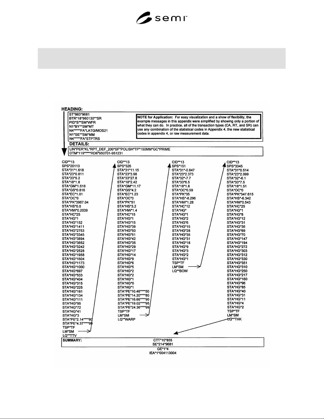
A5-3 Statistical Results Transmission
The "ISA" and "GS" segments indicated at the start of this example and the "GE" and "IEA" segments located at the
end are generally handled by the Information System (IS) dept. in charge of managing the translation and routing of
EDI messages through various VAN channels, and are not part of this document.
ISA*00* *00* *01*9012345720000 *01*908887732000 *960130*2049*U*00200*004113004*0*T*:
GS*RT*901234572000*908887732000*960130*2049*4*T*003050

SEMI T6-0697 © SEMI 1997, 2004 40
NOTICE: SEMI makes no warranties or representations as to the suitability of the standards set forth
herein for any particular application. The determination of the suitability of the standard is solely the
responsibility of the user. Users are cautioned to refer to manufacturer's instructions, product labels,
product data sheets, and other relevant literature, respecting any materials or equipment mentioned herein.
These standards are subject to change without notice.
By publication of this standard, Semiconductor Equipment and Materials International (SEMI) takes no
position respecting the validity of any patent rights or copyrights asserted in connection with any items
mentioned in this standard. Users of this standard are expressly advised that determination of any such
patent rights or copyrights, and the risk of infringement of such rights are entirely their own responsibility.
Copyright by SEMI® (Semiconductor Equipment and Materials
International), 3081 Zanker Road, San Jose, CA 95134. Reproduction of
the contents in whole or in part is forbidden without express written
consent of SEMI.
SEMI T7-0303 © SEMI 1997, 2003 1
SEMI T7-0303
SPECIFICATION FOR BACK SURFACE MARKING OF DOUBLE-SIDE
POLISHED WAFERS WITH A TWO-DIMENSIONAL MATRIX CODE
SYMBOL
This specification was technically approved by the Global Traceability Committee and is the direct
responsibility of the North American Traceability Committee. Current edition approved by the North
American Traceability Committee on November 22, 2002. Initially available at www.semi.org January 2003;
to be published March 2003. Originally published in 1997; previously published November 2002.
1 Purpose
1.1 This specification is intended to provide a marking
symbology that can be used to mark silicon wafers with
no intrusion into the fixed quality area of the wafer.
2 Scope
2.1 This specification defines the geometric and spatial
relationships and content (including the error checking
and correcting code) of a rectangular two-dimensional
(2-D), machine-readable, binary data matrix code
symbol for back surface marking of notched, double-
side polished wafers of silicon which comply with
SEMI M1.15, and other materials with diameters of 300
mm and larger.
2.2 Although this specification does not specify the
marking techniques that may be employed when
complying with its requirements, it is assumed that the
symbol will be obtained by laser scribing individual
dots.
2.3 The matrix code is applicable to a broad range of
wafer products including epitaxial wafers, SOI wafers,
and unpatterned or patterned polished wafers. The
format and algorithms of this code are based on two-
dimensional symbology specified in ISO/IEC 16022.
NOTICE: This standard does not purport to address
safety issues, if any, associated with its use. It is the
responsibility of the users of this standard to establish
appropriate safety health practices and determine the
applicability or regulatory limitations prior to use.
3 Referenced Standards
3.1 SEMI Standards
SEMI AUX001 — List of Vendor Identification Codes
SEMI M1.15 — Standard for 300 mm Polished
Monocrystalline Silicon Wafers (Notched)
SEMI M12 — Specification for Serial Alphanumeric
Marking of Silicon Wafers
3.2 ISO/IEC Standard
1
ISO/IEC 16022 — International Symbology
Specification – Data Matrix
NOTICE: Unless otherwise indicated, all documents
cited shall be the latest published versions.
4 Terminology
4.1 Definitions
4.1.1 alignment bar, of a data matrix code symbol — a
solid line of contiguous filled cells abutting a line of
alternately filled and empty cells [ISO/IEC 16022].
4.1.2 binary values — a dot in the wafer surface
indicates the binary value 1. The absence of a dot, or a
smooth surface surrounding a cell center point indicates
the binary value 0.
4.1.3 border column — the outermost column of a data
matrix code symbol. This column is a portion of the
finder pattern.
4.1.4 border row — the outermost row of a data matrix
code symbol. This row is a portion of the finder pattern.
4.1.5 cell, of a data matrix code symbol — the area
within which a dot may be placed to indicate a binary
value.
4.1.6 cell center point, of an array — the point at
which the centerline of a row intersects the centerline of
a column.
4.1.7 cell spacing, of an array — the (equal) vertical or
horizontal distance between the cell center points of
contiguous cells.
4.1.8 center line, of a row or column — the line
positioned parallel to, and spaced equally between, the
boundary lines of the row or column.
4.1.9 central area, of a cell — the area enclosed by a
circle centered at the cell center point; used by code
readers to sense the binary value of the cell.
1 International Organization for Standardization, ISO Central
Secretariat, 1, rue de Varembé, Case postale 56, CH-1211 Geneva 20,
Switzerland. Telephone: 41.22.749.01.11; Fax: 41.22.733.34.30
Website: http://www.iso.ch