semi合集-English.pdf - 第7552页
SEMI MF1810-0304 © SEMI 2003, 2004 5 RELATED INFORMATION 1 SUMMARY OF MULTI LABORA TORY ROUND ROBIN TEST NOTICE: This related inform ation is not an official part of SEM I MF1810. It was develope d as part of the develop…

SEMI MF1810-0304 © SEMI 2003, 2004 4
sample. The method bias is estimated using the average
range of the location deviations from the target for the
round-robin results or 2.11 defects/cm
2
.
12 Keywords
12.1 defect density; dislocation; grain boundary;
microscopic; polycrystalline imperfection; preferential
etch; silicon; slip
SEMI MF1810-0304 © SEMI 2003, 2004 5
RELATED INFORMATION 1
SUMMARY OF MULTI LABORATORY ROUND ROBIN TEST
NOTICE: This related information is not an official part of SEMI MF1810. It was developed as part of
the development of the document. This related information was approved for publication by full letter
ballot on December 4, 2004.
R1-1 The multilaboratory round robin test was done
over a period of 12 months and included 16
laboratories. The test required each laboratory to
complete 11 diameter scan measurements of seven
wafers. A “diameter scan” area is equal to the area
defined by a microscope field of view and a length
equal to the wafer diameter less the edge exclusion.
Only one defect classification, OISF, was included in
the count and described with pictures. The sequence
and path of the measurement scans were defined so that
the comparison of the individual measurements would
be possible among data sets. Within the ability of each
laboratory to align the sample on the microscope stage,
the starting point and scan path was held constant.
R1-2 The complete repeatability and reproducibility
study results are listed in Table R1-1 for the four scan
method for the parameter, deviation from target, in
units of defects/cm
2
. The average range was 2.107 and
the range of x-bars was 12.130.
Table R1-1 Repeatability and Reproducibility for 16
Laboratories, Seven Samples, and Two Trials
Estimated
Sigma
Estimated
Variance
Percent of
Total
Repeatability 1.863 3.472 23.92
Reproducibility 3.323 11.045 76.08
Repeatability and
Reproducibility
3.810 14.517 100.00
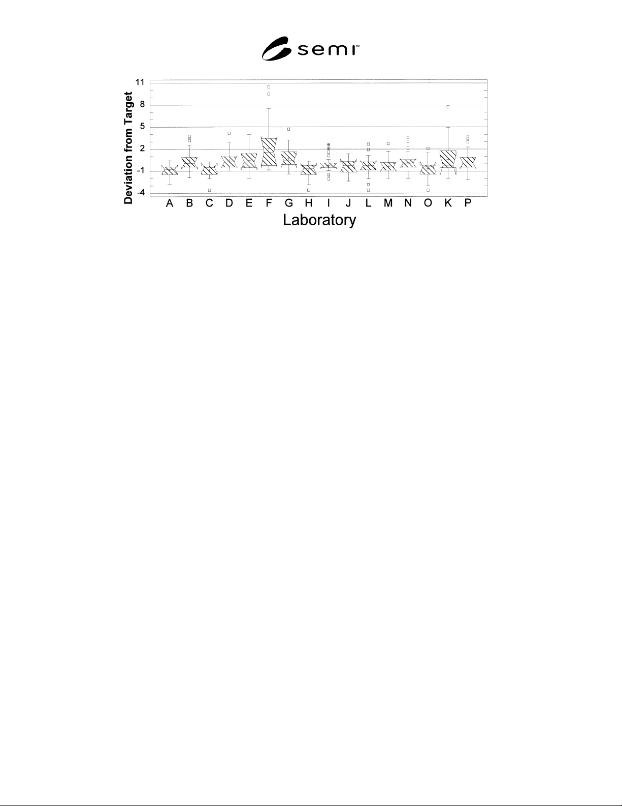
R1-3 A multiple range test by the 95% least squares
deviation (LSD) method for the deviation from target
by laboratory was done. Results are shown in Table
R1-2. Differences among laboratories are also evident
in the 95% confidence interval box and whisker plot
provided in Figure R1-1, which shows the deviation
from target for each laboratory. This plot is based on
four diameter scans per test.
R1-4 Results from Laboratory F were significantly
different from all other laboratories, but were included
in the reported Precision and Bias Section because no
evidence pointed to a procedural mistake. The
alternative repeatability and reproducibility study
results are listed in Table R1-3 for the four scan method
for the parameter, deviation from target, in units of
defects/cm
2
. In this case, the average range was 1.930
and the range of x-bars was 7.018.
Table R1-2 Multiple Range Test for 16 Laboratories
Laboratory Count
Least
Squares
Mean
Homogeneous
Groups
H 77 –0.948022 X
C 77 –0.948002 X
A 77 –0.868478 XX
O 77 –0.635124 XXX
M 77 –0.469934 XX
J 77 –0.437819 X
I 77 –0.28686 XX
L 77 –0.261265 XX
N 77 0.064319 XX
P 77 0.176689 XX
B 77 0.403837 XX
E 77 0.406758 XX
K 77 0.425747 XXX
D 77 0.549704 XX
G 77 0.816097 X
F 77 2.01237 X
Table R1-3 Repeatability and Reproducibility for 16
Laboratories, Seven Samples, and Two Trials
Estimated
Sigma
Estimated
Variance
Percent of
Total
Repeatability 1.707 2.912 44.08
Reproducibility 1.922 3.695 55.92
Repeatability and
Reproducibility
2.570 6.607 100.00
SEMI MF1810-0304 © SEMI 2003, 2004 6
Figure R1-1
95% Confidence Interval Box and Whisker Plot for 16 Laboratories
NOTICE: SEMI makes no warranties or representations as to the suitability of the standards set forth herein for any
particular application. The determination of the suitability of the standard is solely the responsibility of the user.
Users are cautioned to refer to manufacturer' s instructions, product labels, product data sheets, and other relevant
literature, respecting any materials or equipment mentioned herein. These standards are subject to change without
notice.
By publication of this standard, Semiconductor Equipment and Materials International (SEMI) takes no position
respecting the validity of any patent rights or copyrights asserted in connection with any items mentioned in this
standard. Users of this standard are expressly advised that determination of any such patent rights or copyrights, and
the risk of infringement of such rights are entirely their own responsibility.
Copyright by SEMI® (Semiconductor Equipment and Materials
International), 3081 Zanker Road, San Jose, CA 95134. Reproduction o
f
the contents in whole or in part is forbidden without express written
consent of SEMI.