semi合集-English.pdf - 第5865页
SEMI P34-0200 © SEMI 2000 8 A P PENDIX 1 PHOTOMASK FUSED SILICA PROPERTIES NOT E: The ma terial in this appendix is an of ficial part of SEMI P34 and w as appr oved by full letter ballot proc edures on Septem ber 3, 1999…
SEMI P34-0200 © SEMI 20007
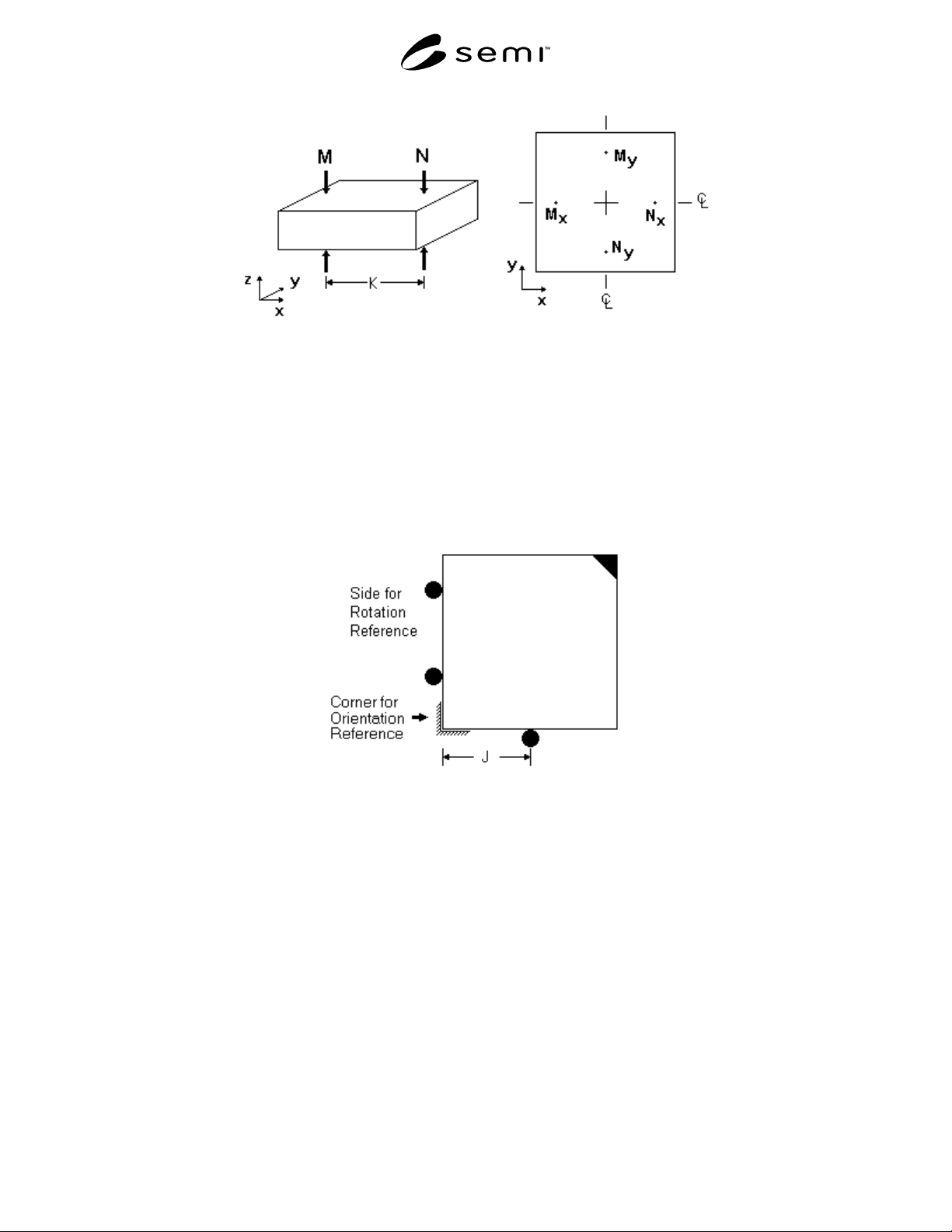
Parallelism = | N
i
– M
i
| for i = x, y
K = 0.7 × edge length N, M within flatness quality area
Figure 7
Measurements for Calculation of Parallelism
with Approximate Positions
J = 115 ± 15 mm
Figure 8
Corner Recommended for Orientation,
Diagonally Opposite of Chamfer (Non-critical Side Shown)
SEMI P34-0200 © SEMI 2000 8
APPENDIX 1
PHOTOMASK FUSED SILICA PROPERTIES
NOTE: The material in this appendix is an official part of SEMI P34 and was approved by full letter ballot procedures on
September 3, 1999 by the North American Regional Standards Committee.
Table A1-1 Fused Silica Properties
Property
ULTRA LOW THERMAL EXPANSION (ULTE)
Modulus of Elasticity 65.7-72.6 GPa
Poisson's Ratio 0.16-0.19
Specific Gravity 2.18-2.20 g/cm
3
Index of Refraction @ λ = 436 nm
1.4667
Index of Refraction @ λ = 365 nm
1.4746
Index of Refraction @ λ = 248 nm
1.5086
Index of Refraction @ λ = 193 nm
1.5608
Thermal Optical Coefficient @ λ = 436 nm 10.6 ppm/°C @ 22°C
Thermal Optical Coefficient @ λ = 365 nm 11.2 ppm/°C @ 22°C
Thermal Optical Coefficient @ λ = 248 nm 14.2 ppm/°C @ 22°C
Thermal Optical Coefficient @ λ = 193 nm 20.6 ppm/°C @ 22°C
NOTE 1: Thermal Optical Coefficient is the same as Temperature Coefficient of Index of Refraction.
NOTICE: SEMI makes no warranties or representations as to the suitability of the standard set forth herein for any
particular application. The determination of the suitability of the standard is solely the responsibility of the user.
Users are cautioned to refer to manufacturer’s instructions, product labels, product data sheets, and other relevant
literature respecting any materials mentioned herein. These standards are subject to change without notice.
The user’s attention is called to the possibility that compliance with this standard may require use of copyrighted
material or of an invention covered by patent rights. By publication of this standard, SEMI takes no position
respecting the validity of any patent rights or copyrights asserted in connection with any item mentioned in this
standard. Users of this standard are expressly advised that determination of any such patent rights or copyrights, and
the risk of infringement of such rights, are entirely their own responsibility.
Copyright by SEMI® (Semiconductor Equipment and Materials
International), 3081 Zanker Road, San Jose, CA 95134. Reproduction o
f
the contents in whole or in part is forbidden without express written
consent of SEMI.

SEMI P35-0704 © SEMI 2000, 2004 1
SEMI P35-0704
TERMINOLOGY FOR MICROLITHOGRAPHY METROLOGY
This standard was technically approved by the Global Micropatterning Committee and is the direct
responsibility of the North American Microlithography Committee. Current edition approved by the North
American Regional Standards Committee on April 22, 2004. Initially available at www.semi.org June 2004;
to be published July 2004 Originally published February 2000; previously published June 2000.
NOTICE: This document was entirely rewritten in
2004.
1 Purpose
1.1 Clear and commonly accepted definitions are
needed for efficient communication and to prevent
misunderstanding between buyers and vendors of
metrology equipment. The purpose of this document is
to provide a consistent terminology for the
understanding and discussion of metrology issues
important to microlithography.
2 Scope
2.1 The scope of this document is limited to the
definitions of metrology terms used in
microlithography. Every attempt is made to keep these
definitions consistent with relevant international
standards and common usage. This document is not
intended to describe a measurement procedure, but
rather an approach to defining a measurand in a useful
and unambiguous way.
2.2 This document does not attempt to discuss
statistical considerations, which are covered in SEMI
E89 and elsewhere.
2.3 This document is expected to grow as more terms
are added in future revisions.
NOTICE: This standard does not purport to address
safety issues, if any, associated with its use. It is the
responsibility of the users of this standard to establish
appropriate safety and health practices and determine
the applicability of regulatory or other limitations prior
to use.
3 Referenced Documents
3.1 SEMI Standards
SEMI P28 — Specification for Overlay-Metrology Test
Patterns for Integrated-Circuit Manufacture
SEMI E89 — Guide for Measurement System
Capability Analysis
3.2 ANSI/NCSL Standards
1
Z540-2-1997 — US Guide to the expression of
Uncertainty in Measurement, ANSI/NCSL standard
(the US version of Guide to the expression of
uncertainty in measurement, ISO, 1995, 110 p., ISBN
92-67-10188-9)
4 Some Metrology Issues
4.1 Measuring Linewidth — Any measurement of
length or position contains an unknown error whose
influence on subsequent application of the measurement
data is best described by the measurement uncertainty
[reference Section 3.2]. The problem of measuring
feature sizes on photomasks or integrated circuit wafers
(e.g., linewidth) is complicated by the fact that a feature
is a 3-dimensional object whose exact shape is
generally not known. The metrology problem is further
complicated when the object is microscopic and only its
magnified image can be measured.
4.2 Feature measurement data are usually reduced to
one or a few parameters because the additional data
needed to describe the complex actual feature shape are
seldom available and may be immaterial to the
subsequent application of the measurement data.
4.3 The first rule of metrology is to define exactly what
is to be measured. The approach used here, in light of
the previous paragraphs, is to construct a simple
idealized geometric shape, or feature model (Figure 1),
which approximates a real object of complex shape.
This model, whose size and center position are well
defined, is substituted for the real feature in application
of the measurement data. A model can be refined to
better approximate the actual feature shape by adding
degrees of freedom, requiring more parameters to
describe the measurement. For example, a line might be
represented by a rectangular cross section (with width
and height) or better represented by a trapezoidal cross
section (with base width, height, and two wall angles).
The differences between the model and the actual shape
of the feature contribute to the overall measurement
uncertainty of the size or position of that feature.
1 American National Standards Institute, Headquarters: 1819 L
Street, NW, Washington, DC 20036, USA. Telephone: 202.293.8020;
Fax: 202.293.9287, New York Office: 11 West 42nd Street, New
York, NY 10036, USA. Telephone: 212.642.4900; Fax:
212.398.0023, Website: www.ansi.org