semi合集-English.pdf - 第7909页
SEMI T14-1104 © SEMI 2004 6 Orien tat ion F idu cial Axi s [011] Notch WAFE R SURFACE 3.0 from Orientation Fiducial Axis Outer periphery of FQA Edge Exclusive Area Edge Profile region Wafer Periphery Orien tat ion F idu …
SEMI T14-1104 © SEMI 2004 5
6.0 µm
+10%
-20%
+10%
-20%
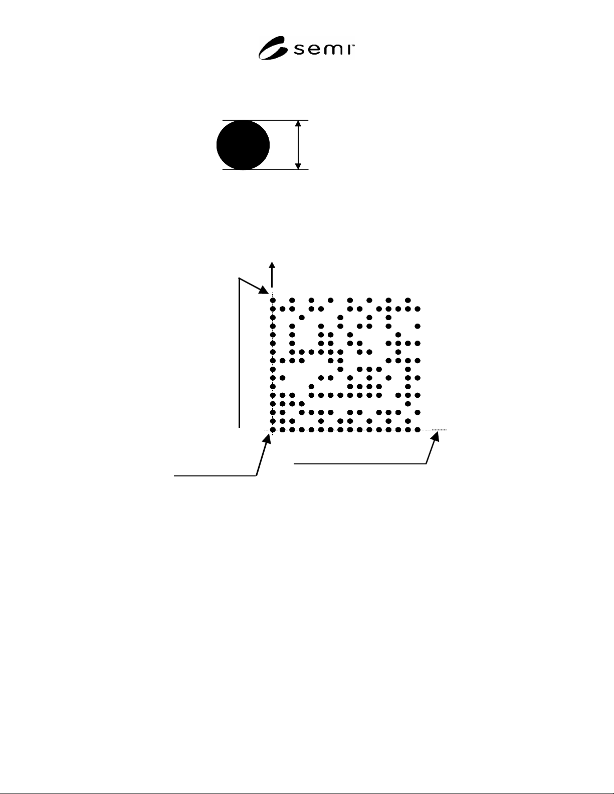
Figure 3
Dot Shape Circle (Projected Sectional Area)
To Wafer Center
Reference Point
The Primary Border Row
The Primary Border Column
Figure 4
Data Matrix Code Fields
ECC200 - 16 rows × 16 columns
SEMI T14-1104 © SEMI 2004 6
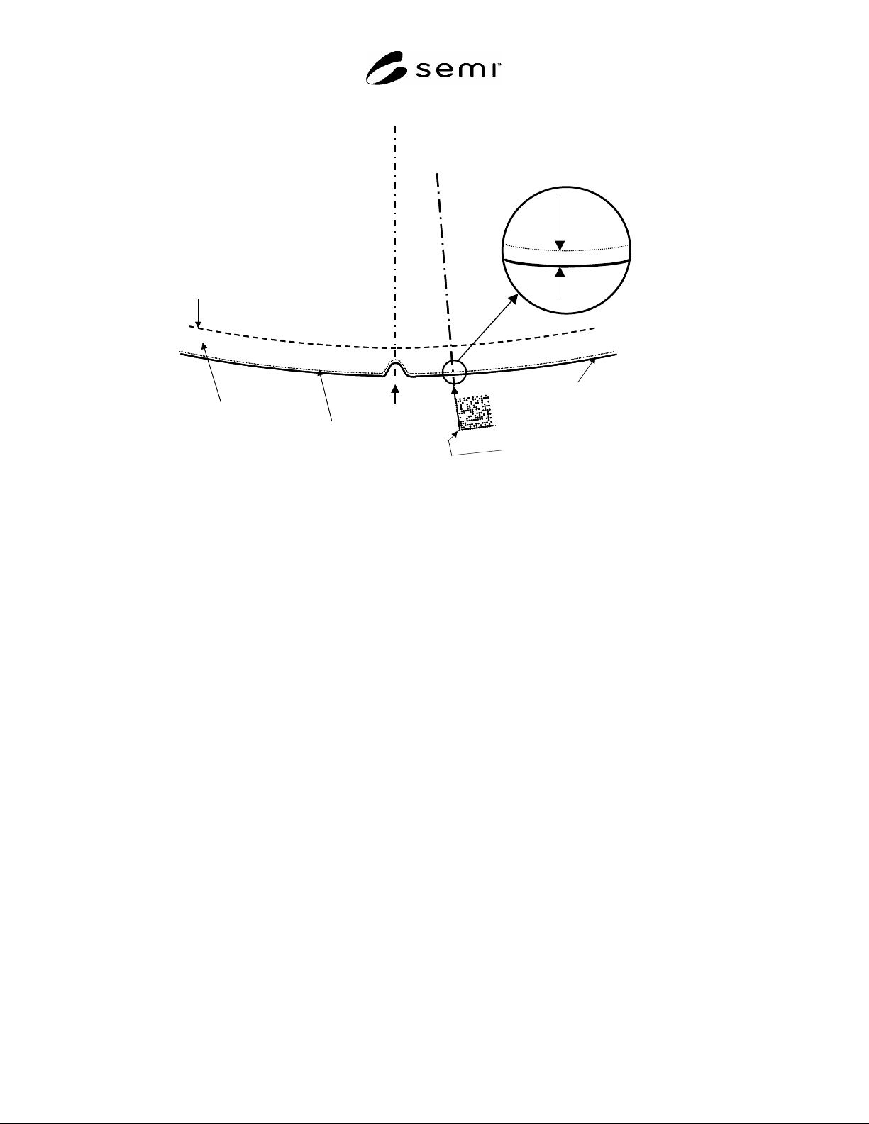
Orientation Fiducial Axis
[011]
Notch
WAFER SURFACE
3.0 from
Orientation Fiducial Axis
Outer periphery of FQA
Edge Exclusive Area
Edge Profile region
Wafer Periphery
Orientation Fiducial Axis
[011] ± 1.0°
Notch
WAFER SURFACE
3.0 ± 0.1° from
Orientation Fiducial Axis
Outer periphery of FQA
Edge Exclusive Area
Edge Profile region
Wafer Periphery
R
e
f
e
r
e
n
c
e
P
o
i
n
t
ID Mark Area
NOTE: Figure 5 is not to scale.
Figure 5
Data Matrix Code Location on Front Bevel Surface of Notched 300 mm Diameter Wafer
Top View
SEMI T14-1104 © SEMI 2004 7
RELATED INFORMATION 1
APPLICATION NOTES
NOTICE: This related information is not an official part of SEMI (doc#) and was derived from the Japanese
Traceability committee. This related information was approved for publication by full letter ballot on July 23, 2004.
R1-1 Shape and Size of the Protrusion Dot Mark
R1-1.1 A microdot mark is formed by laser irradiation and consists of a single dot mark on each laser-irradiated
point. The mark has a single protrusion, which includes a concave portion provided around the protrusion and lower
than a surface of the wafer and whose center potion protrudes upward so as to be higher than the surface of the
wafer. The length of each dot mark along the surface of the article to be marked should be 6.0 µm + 10% – 20%.
The protrusion height is more than 300 nanometers, formed on each laser irradiate point. (As shown in below Figure
R1-1.)
+10%
- 20%
A
A
A-A
H 300 nm
>
=
6.0 µm
H
NOTE: Figure R1-1 is not to scale.
Figure R1-1
Dot Height & Vertical Cross Section
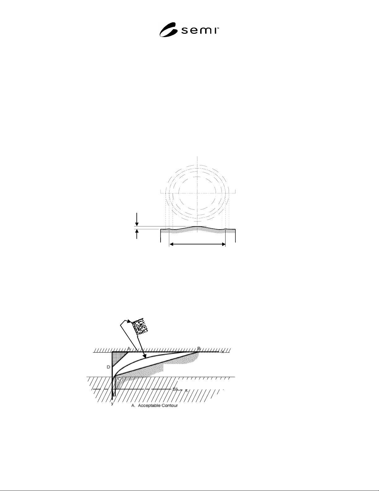
R1-2 Location of Data Matrix Code Symbol
R1-2.1 Data matrix code location is defined on the front bevel of a 300 mm diameter notched wafer, whose side
view is referred from SEMI M1.
Back Grinded area
Polished Area by
Chemical Mechanical Polishing (CMP)
Remaining area for Micro ID
R
e
f
e
r
e
n
c
e
P
o
i
n
t
NOTE: Figure R1-2 is not to scale.
Figure R1-2
Data Matrix Code Location on Front Bevel Surface of 300 mm Diameter Wafer
Side View