semi合集-English.pdf - 第6097页
SEMI G19-0997 © SE MI 1980, 1997 2 Figure 4 Undercut and Etch Factor functional ar ea — The die attach pad and w ire bond (lead tip) area. lateral et ch or undercut — T he allow able bevelled edge caused by the leadframe…
SEMI G19-0997 © SEMI 1980, 19971
SEMI G19-0997
SPECIFICATION FOR DIP LEADFRAMES PRODUCED BY ETCHING
1 Preface
This specification is a guideline for production of DIP
leadframes for plastic molded semiconductor packages
produced by the etching process. It is a design guideline
for packaging engineers, etchers, and mold
manufacturers and has been developed to meet the
requirements of automatic bonders.
2 Applicable Documents
2.1 SEMI Standards
SEMI G18 — Specification for Integrated Circuit
Leadframe Material Used in the Production of Etched
Leadframes
SEMI G10 — Standard Method for Mechanical
Measurement of Plastic Package Leadframes
2.2 Other Document
PCM1 D-300
1
— Standard Specification
3 Selected Definitions
burrs and protrusions — Fragments of excess material,
either horizontal or vertical, attached to the lead frame.
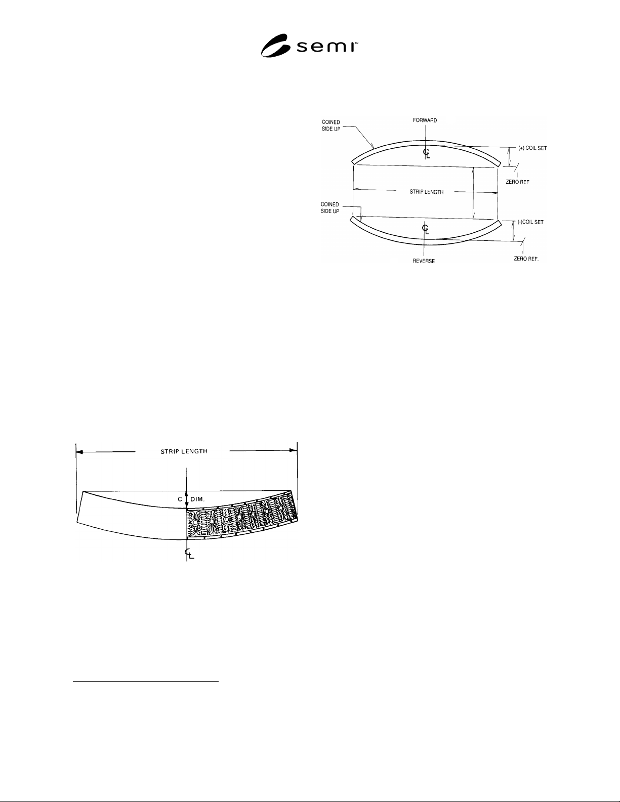
camber — Curvature of the leadframe strip edge (see
Figure 1).
Figure 1
Camber
coil set — Longitudinal bowing of the leadframe (see
Figure 2).
1 Photochemical Machining Institute, 4113 Barberry, Lafayette Hills,
PA 19444
Figure 2
Coil Set
compensation — Changes made in the dimensions on
the master artwork other than those specified on the
engineering artwork that allow for the process variables
(i.e., etch factor, undercut).
crossbow — Transverse bowing of the leadframe (see
Figure 3).
(enter graphic when available)
Figure 3
Crossbow
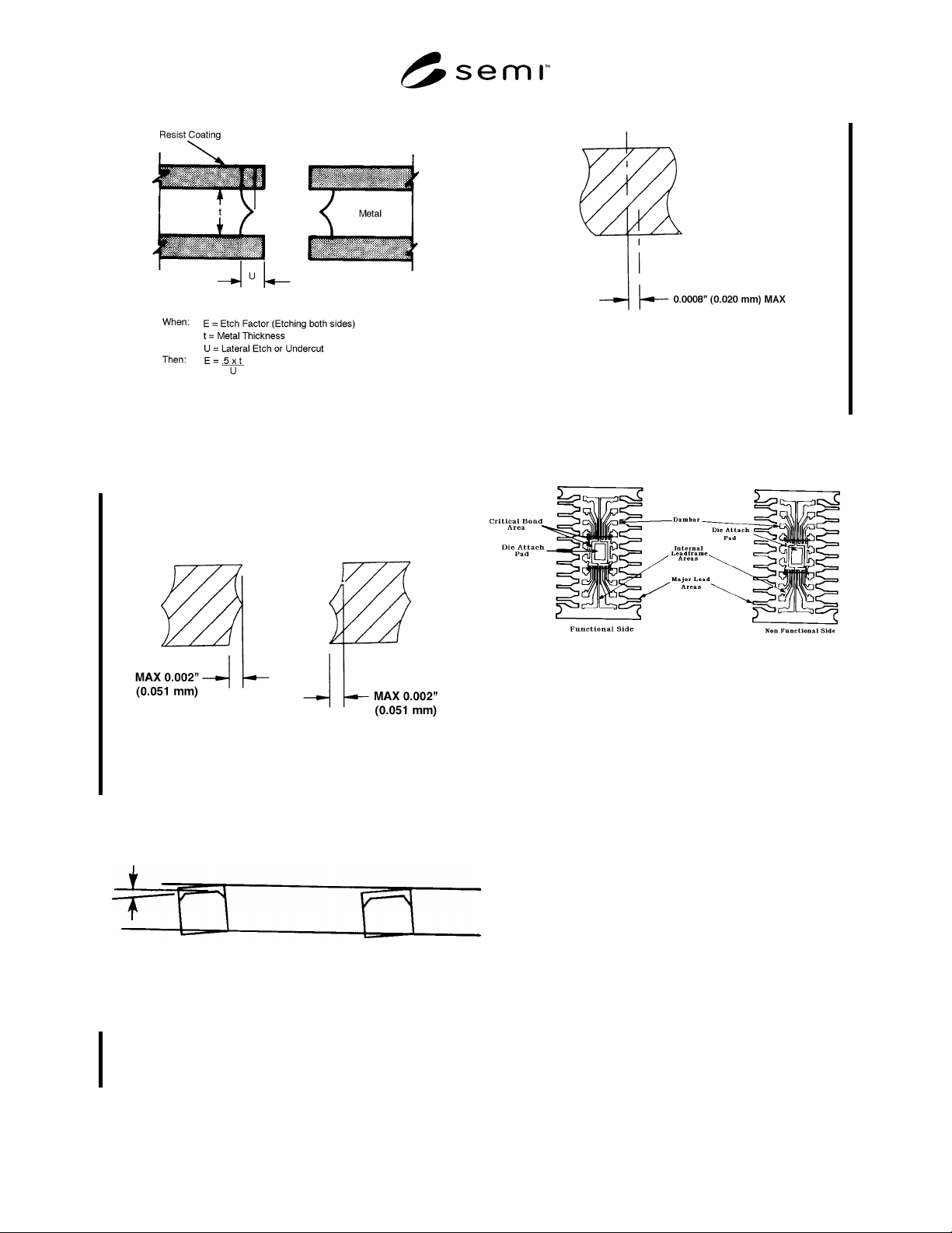
etch factor — The ratio of etched depth to the lateral
etch or undercut (see Figure 4).
SEMI G19-0997 © SEMI 1980, 1997 2
Figure 4
Undercut and Etch Factor
functional area — The die attach pad and wire bond
(lead tip) area.
lateral etch or undercut — The allowable bevelled edge
caused by the leadframe etchant attacking the metal
laterally as well as vertically (see Figure 5).
Figure 5
Overetching
lead twist — Angular rotation of the bond fingers (see
Figure 6).
Figure 6
Lead Twist
offset alignment accuracy — The top to bottom
alignment accuracy of the etched leadframe operation
(see Figure 7).
Figure 7
Etched Offset
pits — Shallow surface depressions or craters in the
leadframe material (see Figure 8).
Figure 8
Pits
resist breakdown — Etching under the edges of the
resist causing more than a standard undercut.
undercut — Bevelled edge caused by the etchant
attacking the metal laterally as well as vertically (see
Figure 4).
4 Ordering Information
Purchase orders for leadframes for plastic molded
semiconductor packages furnished to this specification
shall include the following items:
1. Drawing number and revision level
2. Material
3. Number of leads
4. Material certification
5. Number of units/strip
6. Plating requirements
7. Packaging and marking (see Section 8)
SEMI G19-0997 © SEMI 1980, 19973
5 Dimensions
See applicable leadframe drawing as referred to in the
ordering information.
6 Defect Limits and Parame ters (see SEMI
G10 to Measure)
6.1 Minimum Flat Wire Bonding Area — 0.203 mm
(0.008") or 80% of nominal lead width, whichever is
greater in width and 0.635 mm (0.025") in length.
Undercut is an unavoidable process of etching. The
above parameters are applicable only so long as the flat
surface area is obtainable using the formula of Figure 4.
The “radiusing” effect of the etching process will round
off the tips and, therefore, the length of the flat area
should be measured by starting back from the tip 0.254
mm (0.010").
NOTE: 0.008" flat is desirable. In order to achieve 0.008" flat,
on 0.010" thick material, it is necessary to have a design
width of 0.022" center to center, giving a 0.012" wide lead
and 0.010" wide space.
6.2 Horizontal Lead Spacing and Location
6.2.1 Spacing between leads to be 0.152 mm (0.006")
minimum after plating.
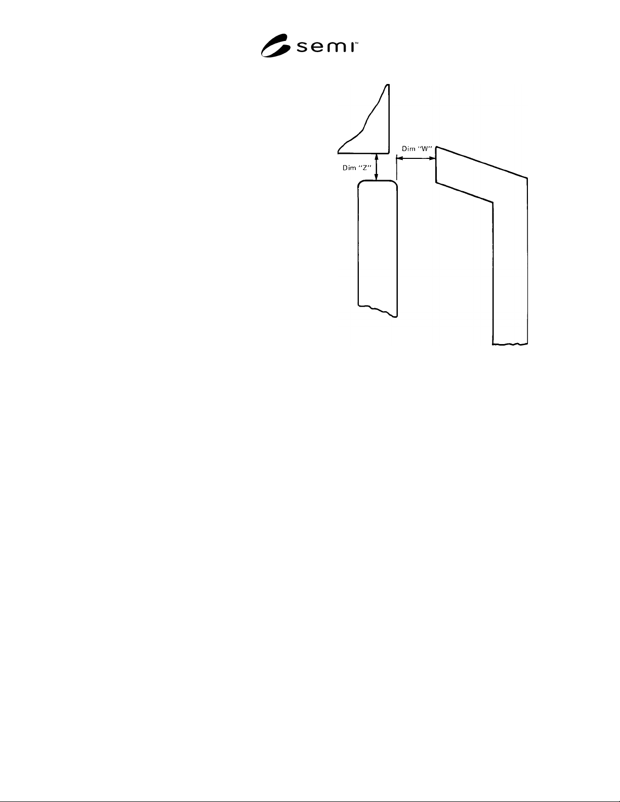
6.2.2 Metal to metal clearance (Dimension “W”
Figure 7) minimum clearance shall be the greater of
0.152 mm (0.006") or the drawing dimension “W”
minus 0.102 mm (0.004"). In determining dimension
“W,” the tolerance limits (max. vs. min.) shown on the
drawing shall be used in the calculation.
Figure 7
Metal to Metal Clearance
6.3 Lead Twist — Not to exceed 2° 30' or 0.0004"
(0.010 mm) per 0.010" (0.254 mm) of lead width.
6.4 Die Attach Pad Tilt & Flatness
6.4.1 Tilt — 0.001" (0.025 mm) maximum per 0.100"
(2.54 mm) of length or width in the undepressed state
and 0.002" (0.050 mm) max per 0.100" (2.54 mm) of
length or width in the depressed state when measuring
from corner to corner. The corners are defined as
0.005" (0.127 mm) from each edge.
6.4.2 Flatness — 0.0004" (0.010 mm) maximum
difference per 0.100" (2.54 mm) of length or width
when measuring from center to average of four corners.
The corners are defined as 0.005" (0.127 mm) from
each edge.
6.5 Die Attach Pad Offset or Depression — (if
applicable) — ± 0.002" (0.050 mm) as measured from
the center of the pad to a point on the bar pad support
strip. The nominal recommended offset is 0.015" (0.381
mm).
6.6 Lead and Die Attach Pad Coplanarity — See
SEMI G10 for measurement procedure.
6.6.1 Lead Planarity — The lead tips as measured in
the center of the flat wirebonding area must be within
the following tolerances of the “Z” plane. Use Table 1