semi合集-English.pdf - 第5033页
SEMI M18-0704 © SEMI 1990, 2004 19 Roughness (Si surface) rms @ 10 × 10 µ m ≤ [ ] (nm) 100243 Test Method [ ] Atomic force microscope, [ ] Others: Roughness (Si surface) rms@ [ ] × [ ] µ m ≤ [ ] (nm) 100244 Test Method […
SEMI M18-0704 © SEMI 1990, 2004 18
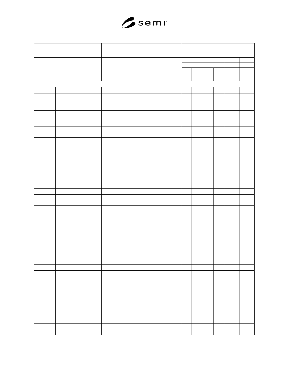
Part 6 SOI wafers for CMOS LSI Applications
CUSTOMER:
PART NUMBER:
REVISION
DATE:
TESTING LEVEL EDI Sub
WAFER
TEST PIECE
Code Param
REQUIRED
ITEM
SPECIFICATION
100%
SAMP
LE
100%
SAMP
LE
ID ID
25. SOI LAYER CHARACTERISTICS
♦
25.0 Type of SOI [ ] SIMOX [ ] Bonded 100226
25.1 Starting silicon wafer for
SOI
[ ] Polished [ ] Epitaxial [ ]Others 100227
♦
25.2 Surface Silicon Thickness [ ] (nm) See NOTE 8 100228
Test Method [ ] Spectroscopic ellipsometry
[ ] Spectroscopic reflectometry
[ ] Others
25.3 Surface Silicon Thickness
Mean Value Variation
≤ ± [ ] (nm) See NOTE 9
100229
Test Method [ ] Spectroscopic ellipsometry
[ ] Spectroscopic reflectometry
[ ] Others
♦
25.4 Surface Silicon Thickness
Variation in Wafer
[ ] ≤ ± [ ] (%)
[ ] ≤ ± [ ] (nm)
See NOTE 9
100230
25.5 Crystal Orientation
(100) ± [ ] (degree)
100231
Test Method [ ] X-ray diffraction, [ ] Others:
25.6 Rotation Misalignment
≤ ± [ ] (degree) for Bonded
100232
Test Method [ ] Visual, [ ] Others:
25.7 Edge Exclusion,
Nominal
[ ] (mm) See NOTE 10 100233
25.8 Non-SOI Edge Area
≤ [ ] (mm) for Bonded
100234
Test Method [ ] Visual, [ ] Others:
25.9 Conductivity Type [ ]P-type [ ]N-type 100235
25.10 Dopant [ ]B [ ]P [ ]Others: 100236
Test Method [ ] Secondary ion mass spectroscopy,
[ ] Others
25.11 Dopant Concentration [ ] (atoms /cm
3
) See NOTE 8 100237
Test Method [ ] Secondary ion mass spectroscopy,
[ ] Others:
25.12 SOI Etch Pit
≤ [ ] (/cm
2
)
100238
Test Method [ ] Secco's Etching, [ ] Others:
25.13 Threading Dislocation
≤ [ ] (/cm
2
) for SIMOX
100239
Test Method [ ] Secco's Etching, [ ] Others:
25.14 HF Defect ≤ [ ] (/cm
2
) 100240
Test Method [ ] HF Etching, [ ] Others:
25.15 Void ≤ [ ] (/wafer) for Bonded 100241
Test Method [ ] Automated particle counter,
[ ] Visual, [ ] Others:
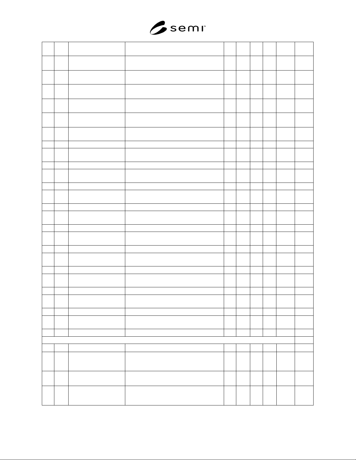
25.16 Roughness (Si surface)
rms @ 2 × 2µm
≤ [ ] (nm) 100242
Test Method
[ ] Atomic force microscope,
[ ] Others:
SEMI M18-0704 © SEMI 1990, 2004 19
Roughness (Si surface)
rms @ 10 × 10µm
≤ [ ] (nm) 100243
Test Method
[ ] Atomic force microscope,
[ ] Others:
Roughness (Si surface)
rms@ [ ] × [ ]µm
≤ [ ] (nm) 100244
Test Method
[ ] Atomic force microscope,
[ ] Others:
Roughness (Si surface)
rms@ [ ] × [ ]µm
≤ [ ] (nm) 100245
Test Method
[ ] Atomic force microscope,
[ ] Others:
25.17 Surface Metal (Fe)
Contamination
≤ [ ] (/cm
2
) 100246
Test Method [ ] TXRF, [ ] AAS, [ ] ICP-MS
Surface Metal (Cr)
Contamination
≤ [ ] (/cm
2
) 100247
Test Method [ ] TXRF, [ ] AAS, [ ] ICP-MS
Surface Metal (Ni)
Contamination
≤ [ ] (/cm
2
) 100248
Test Method [ ] TXRF, [ ] AAS, [ ] ICP-MS
Surface Metal (Cu)
Contamination
≤ [ ] (/cm
2
) 100249
Test Method [ ] TXRF, [ ] AAS, [ ] ICP-MS
Surface Metal [ ]
Contamination
≤ [ ] (/cm
2
) 100250
Test Method [ ] TXRF, [ ] AAS, [ ] ICP-MS
Surface Metal [ ]
Contamination
≤ [ ] (/cm
2
) 100251
Test Method [ ] TXRF, [ ] AAS, [ ] ICP-MS
Surface Metal [ ]
Contamination
≤ [ ] (/cm
2
) 100252
Test Method [ ] TXRF, [ ] AAS, [ ] ICP-MS
Surface Metal [ ]
Contamination
≤ [ ] (/cm
2
) 100253
Test Method [ ] TXRF, [ ] AAS, [ ] ICP-MS
Surface Metal [ ]
Contamination
≤ [ ] (/cm
2
) 100254
Test Method [ ] TXRF, [ ] AAS, [ ] ICP-MS
Surface Metal [ ]
Contamination
≤ [ ] (/cm
2
) 100255
Test Method [ ] TXRF, [ ] AAS, [ ] ICP-MS
26. BOX CHARACTERISTICS
♦
26.1 BOX Thickness [ ] (nm) See NOTE 8 100256
Test Method [ ] Spectroscopic ellipsometry,
[ ] Spectroscopic reflectometry,
[ ] Others
♦
26.2 BOX Thickness Variation [ ] ≤ ± [ ] (nm),
[ ] ≤ ± [ ] (%)
100257
Test Method [ ] Spectroscopic ellipsometry,
[ ] Spectroscopic reflectometry,
[ ] Others:
SEMI M18-0704 © SEMI 1990, 2004 20
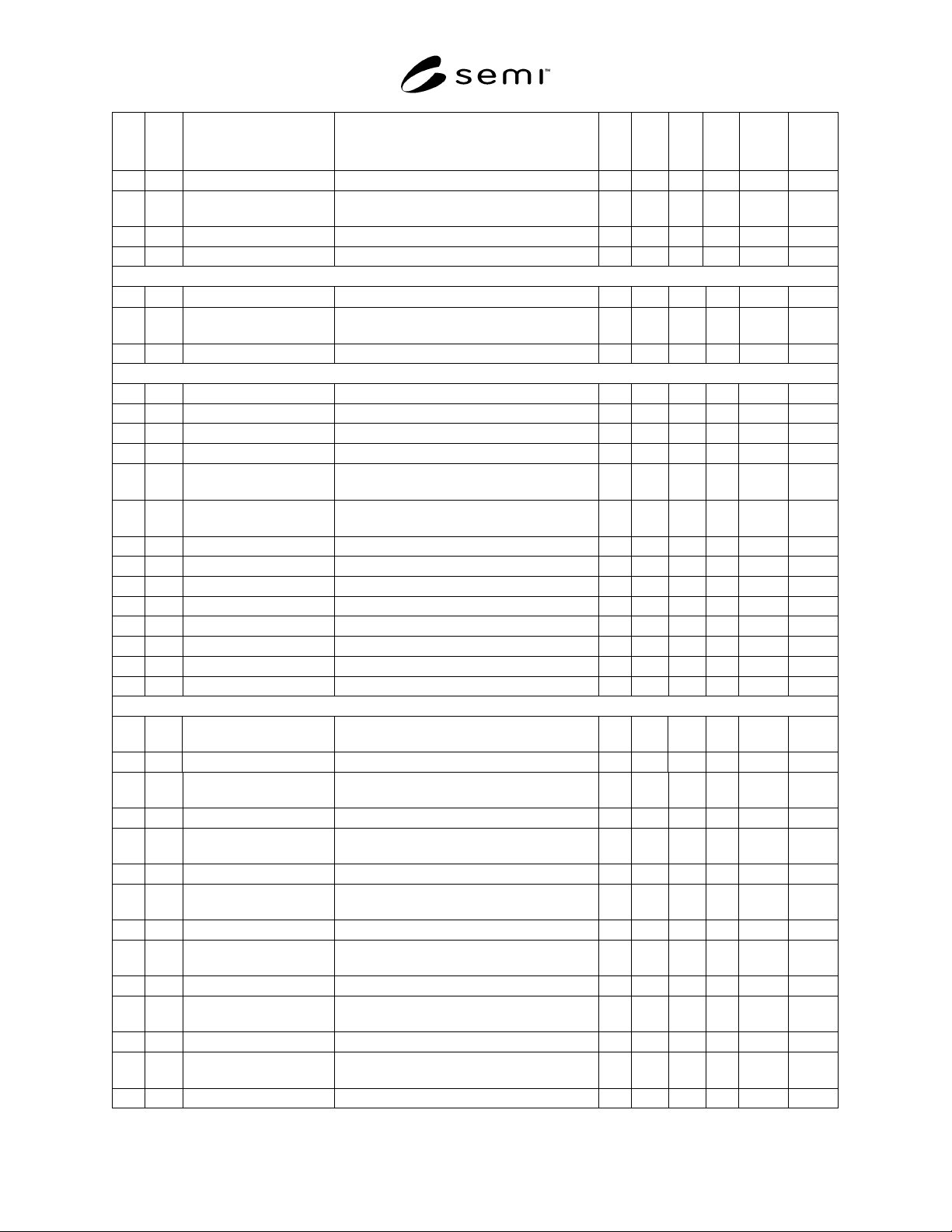
26.3 Bonded Interface
Location
[ ] at SOI/BOX interface
[ ] within BOX layer
[ ] at BOX/Substrate interface
100258
26.4 BOX Pinholes ≤ [ ] (/cm
2
) 100259
Test Method [ ] Cu plating,
[ ] BOX capacitor, [ ] Others:
26.5 Dielectric Breakdown > [ ] (MV/cm) 100260
Test Method [ ] BOX capacitor, [ ] Others:
27. MECHANICAL CHARACTERISTICS
27.1 Warp
≤ [ ] (µm)
100261
Test Method [ ] Automated noncontact scanning
[ ] Others:
27.2 Flatness-site See NOTE 8 100262
28. FRONT SURFACE INSPECTION CHARACTERISTICS
28.1 Scratch None 100263
Test Method [ ] Visual, [ ] Others:
28.2 Haze None 100264
Test Method [ ] Visual, [ ] Others:
28.3 LLS
@particle size
≤ [ ] (/cm
2
)
@ ≥ [ ] (µm)
100265
100266
Test Method [ ] Automated particle counter
[ ] Others:
28.4 Slip See NOTE 8 100267
Test Method [ ] Visual, [ ] Others:
28.5 Edge Chip [ ]SEMI M1, [ ]Others: 100268
Test Method [ ] Visual, [ ] Others:
28.6 Edge Crack [ ]SEMI M1, [ ]Others: 100269
Test Method [ ] Visual, [ ] Others:
28.7 Foreign Matter See NOTE 8 100270
Test Method [ ] Visual, [ ] Others:
29. BACK SURFACE CHARACTERISTICS
29.1 Backside Metal (Fe)
Contamination
≤ [ ] (/cm
2
) for each atom 100271
Test Method [ ] TXRF, [ ] AAS, [ ] ICP-MS
Backside Metal (Cr)
Contamination
≤ [ ] (/cm
2
) 100272
Test Method [ ] TXRF, [ ] AAS, [ ] ICP-MS
Backside Metal (Ni)
Contamination
≤ [ ] (/cm
2
) 100273
Test Method [ ] TXRF, [ ] AAS, [ ] ICP-MS
Backside Metal (Cu)
Contamination
≤ [ ] (/cm
2
) 100274
Test Method [ ] TXRF, [ ] AAS, [ ] ICP-MS
Backside Metal [ ]
Contamination
≤ [ ] (/cm
2
) 100275
Test Method [ ] TXRF, [ ] AAS, [ ] ICP-MS
Backside Metal [ ]
Contamination
≤ [ ] (/cm
2
) 100276
Test Method [ ] TXRF, [ ] AAS, [ ] ICP-MS
Backside Metal [ ]
Contamination
≤ [ ] (/cm
2
) 100277
Test Method [ ] TXRF, [ ] AAS, [ ] ICP-MS