semi合集-English.pdf - 第5756页
SEMI P19-92 © SEMI 19 92, 1996 7 3.2.7.5 The pads can be arran ged in a 1 × n la yout for scribeli ne placem e nt (see Fi gure 15), or the conve ntio nal 2 × n layo ut ca n be used if the sp atia l constraints are minima…
SEMI P19-92 © SEMI 1992, 1996 6
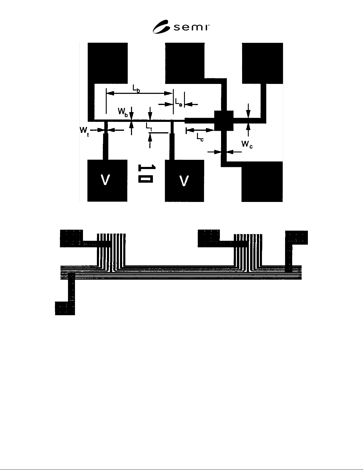
Figure 13
Electrical Cell, 2 × n Configuration with Labeling
Figure 14
Blow-Up of Bridge Resistor with Proximity Lines
SEMI P19-92 © SEMI 1992, 19967
3.2.7.5 The pads can be arranged in a 1 × n layout for
scribeline placement (see Figure 15), or the
conventional 2 × n layout can be used if the spatial
constraints are minimal. Pad size and pitch are user-
defined. For automatic testing in a production
environment, it is recommended that the pads be 80 –
100 mm per side.
3.3 User Considerations
3.3.1 Target CD versus Resolved CD
3.3.1.1 The desired size of a critical d imension (CD)
on an integrated circuit can be considered its nominal
value and is herein designated the “target CD.” The size
actually achieved (resolved CD) on the circuit may be
different from this nominal value.
3.3.1.2 Measurements of the resolved CD may not be
accurate because of the difficulty in determining the
actual location of the edge in the optical or SEM image
profile.
3.3.1.3 Even if inaccurate, measurement of the
resolved CD can be valuable for comparison purposes if
the measurement method has adequate precision and
sensitivity to detect the dimensional changes of interest.
3.3.1.4 The traditional definition of re solution may not
be adequate (e.g., ability to distinguish closely spaced
points) for specifying the sensitivity to small
dimensional changes.
4 References
4.1 Yen, D., Linholm, L.W., and Buehler, M.G., “A
Cross-Bridge Test Structure for Evaluating the
Linewidth Uniformity of an Integrated Circuit
Lithography System,” J. Electrochemical Society
1_2_9_ (1982), 2313.
4.2 Hasan, T.F., Perloff, D.S., and Mallory, C.L.,
“Test Structures for the Measurement and Analysis of
VLSI Lithographic and Etching Parameters”,
Semiconductor Silicon/1981, H.R. Huff, R.J. Kriegler
and Y. Takeishi Eds., (Electrochemical Society,
Pennington, NJ) 1981, 866.
4.3 Carver, G.P., Mattis, R.L., and Buehler, M.G.,
“Design Considerations for the Cross-Bridge Sheet
Resistor,” NBSIR 82-2548, National Bureau of
Standards, Washington, DC, (1982).
4.4 Buehler, M.G., Hershey, C.W. , “The Split-Cross-
Bridge Resistor for Measuring the Sheet Resistance,
Linewidth, and Line Spacing of Conducting Layers,”
IEEE Transactions on Electron Devices, (1986), 1572.
4.5 Lin, Burn J., “Proximity and Astigmatism Tolerant
Testsites for Electrical Linewidth Measurement,” SPIE
Proc., Vol. – (1989).
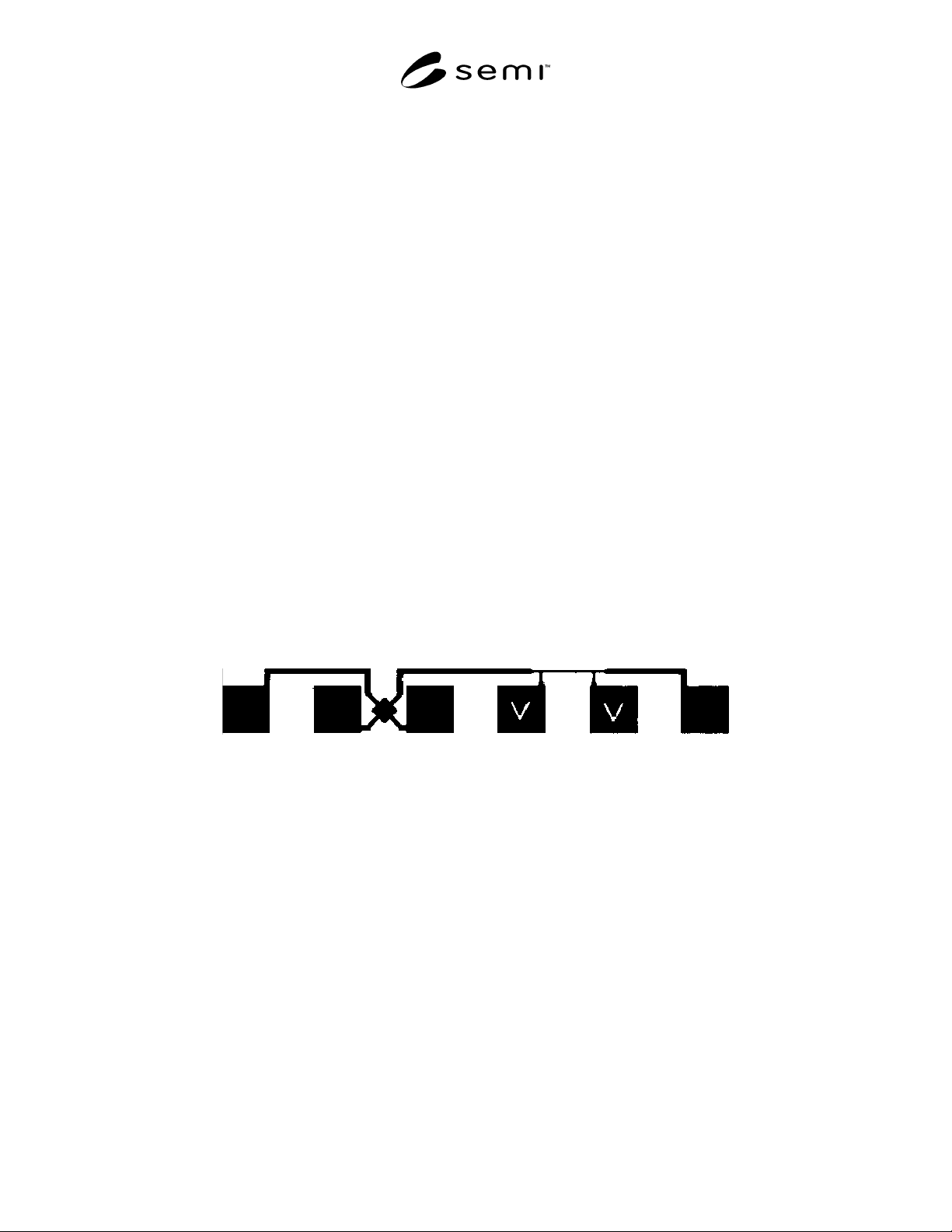
Figure 15
Electrical Cell, 1 × n Configuration
SEMI P19-92 © SEMI 1992, 1996 8
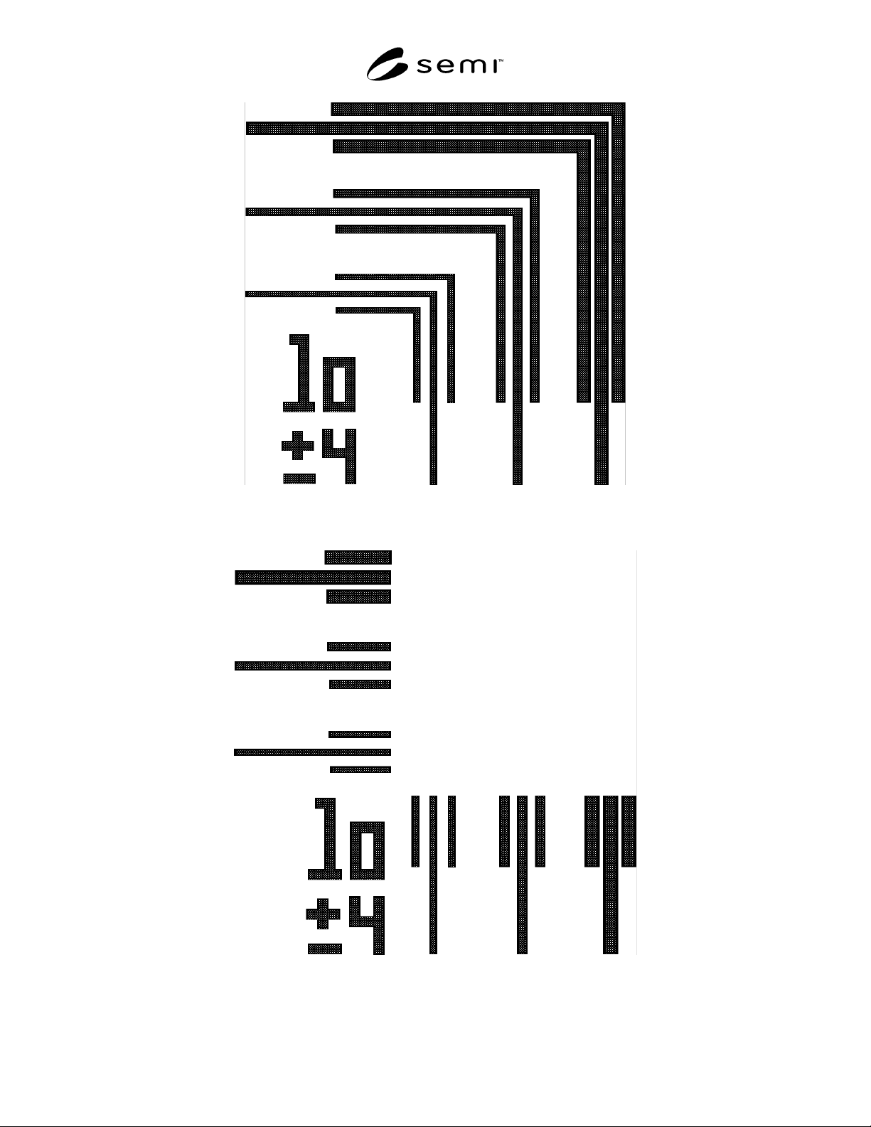
Figure 4
L-Bar Cell
Figure 6
Straight Line Cell