semi合集-English.pdf - 第7385页
SEMI MF1526-95 © SEMI 2004 1 SEMI MF1526-95 (Withdrawn 1104) Test Method for Measuring Surface Metal Contamination on Silicon Wafers by Total Reflection X-Ray Fluorescence Spectroscopy This standard was originally publis…
SEMI MF1451-0704 © SEMI 2004 8
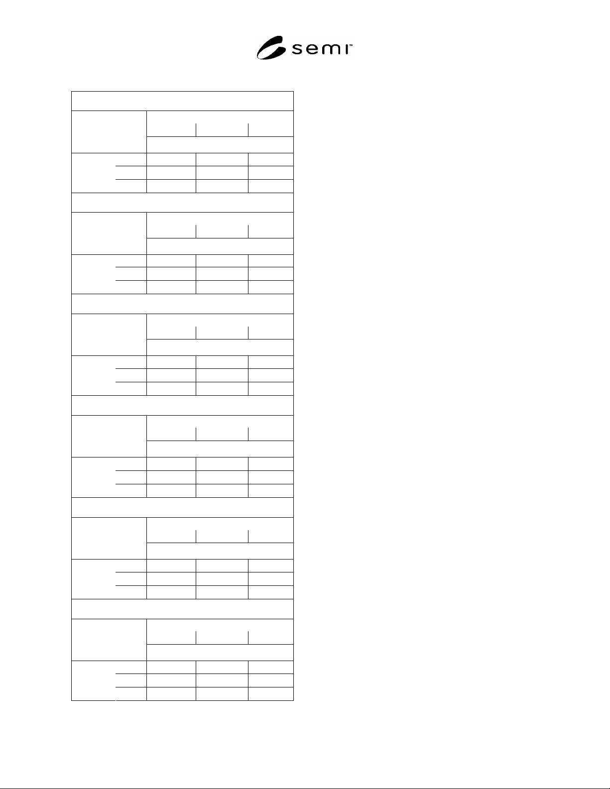
Table R1-2 Examples of Gravity Effect Errors
NOTICE: SEMI makes no warranties or
representations as to the suitability of the standards set
forth herein for any particular application. The
determination of the suitability of the standard is solely
the responsibility of the user. Users are cautioned to
refer to manufacturer's instructions, product labels,
product data sheets, and other relevant literature,
respecting any materials or equipment mentioned
herein. These standards are subject to change without
notice.
By publication of this standard, Semiconductor
Equipment and Materials International (SEMI) takes no
position respecting the validity of any patent rights or
copyrights asserted in connection with any items
mentioned in this standard. Users of this standard are
expressly advised that determination of any such patent
rights or copyrights, and the risk of infringement of
such rights are entirely their own responsibility.
300 mm Diameter Wafers
Actual Diameter, mm
299.8 300.0 300.2
Gravity Effect Errors,
m
755 3.90 5.67 5.96
775
1.68
0.00 0.28
Actual
Thickness,
m
795
6.84 5.25 4.98
200 mm Diameter Wafers
Actual Diameter, mm
199.8 300.0 200.2
Gravity Effect Errors,
m
705 0.77 1.37 1.47
725
0.57
0.00 0.10
Actual
Thickness,
m
745
0.52 1.26 1.17
150 mm Diameter Wafers
Actual Diameter, mm
149.8 150.0 150.2
Gravity Effect Errors,
m
655 0.49 0.54 0.59
675
0.05
0.00 0.05
Actual
Thickness,
m
695
0.54 0.49 0.45
150 mm Diameter Wafers
Actual Diameter, mm
149.8 150.0 150.2
Gravity Effect Errors,
m
610
0.45
0.51 0.56
625
0.05
0.00 0.05
Actual
Thickness,
m
640
0.52 0.47 0.42
125 mm Diameter Wafers
Actual Diameter, mm
124.5 125.0 125.5
Gravity Effect Errors,
m
605 0.25 0.33 0.41
625
0.08
0.00 0.08
Actual
Thickness,
m
645
0.37 0.30 0.22
100 mm Diameter Wafers
Actual Diameter, mm
99.5 100.0 100.5
Gravity Effect Errors,
m
505 0.17 0.23 0.29
525
0.06
0.00 0.06
Actual
Thickness,
m
545
0.26 0.20 0.15
Copyright by SEMI® (Semiconductor Equipment and Materials
International), 3081 Zanker Road, San Jose, CA 95134. Reproduction of
the contents in whole or in part is forbidden without express written
consent of SEMI.

SEMI MF1526-95 © SEMI 2004 1
SEMI MF1526-95 (Withdrawn 1104)
Test Method for Measuring Surface Metal Contamination on Silicon Wafers
by Total Reflection X-Ray Fluorescence Spectroscopy
This standard was originally published by ASTM International as ASTM F 1526-94. It was formally approved by ASTM
balloting procedures and adhered to ASTM patent requirements. Though ownership of this standard has been transferred
to SEMI, it has not been formally approved by SEMI balloting procedures and does not adhere either to SEMI
Regulations dealing with patents or to SEMI Editorial Guidelines. Available at www.semi.org September 2004, to be
published November 2004. Last published by ASTM International as ASTM F 1526-95 (Reapproved 2000).
NOTICE: This document was balloted and approved for withdrawal in 2004.
1. Scope
1.1 This test method covers the quantitative determination of elemental areal density on the surface of polished single
crystal silicon substrates using total reflection X-ray fluorescence spectroscopy (TXRF
1
) with a monochromatic X-ray
source.
2
1.2 This test method can be used for both n-type and p-type silicon.
1.3 This test method can be used to detect surface elemental contamination that is within the analyte depth of approximately
5 nm for highly mirror-polished silicon wafers. The analytic depth increases with surface roughness.
3
1.4 This test method is especially useful for determining the surface elemental areal densities in the native oxide or in
chemically grown oxide of polished silicon wafers after cleaning.
1.5 This test method is useful for elemental areal densities between 10
9
and 10
15
atoms/cm
2
within the measurement area.
See Annex A1 for a discussion of the relationship between repeatability and detection limit.
1.6 This test method is useful for detecting elements with atomic number between 16 (S) and 92 (U), depending upon the
X-ray source provided in the instrument. This test is especially useful for detecting the following metals or elements:
potassium, calcium, titanium, vanadium, chromium, manganese, iron, cobalt, nickel, copper, zinc, arsenic, molybdenum,
palladium, silver, tin, tantalum, tungsten, platinum, gold, mercury, and lead.
1.7 The detection limit depends upon atomic number, excitation energy, photon flux of excitation X-rays, instrumental
background, integration time, and blank value. For constant instrumental parameters, the interference-free detection limits
vary over two orders of magnitude as a function of atomic number of the element.
1.8 This test method is nondestructive.
1.9 This test method is complementary to a variety of other test methods:
1.9.1 Electron spectroscopy for chemical analysis that can detect elemental surface areal densities down to the order of 10
13
atoms/cm
2
.
1.9.2 Auger electron spectroscopy that can detect elemental surface areal densities down to the order of 10
2
atoms/cm
2
.
1.9.3 Nitrogen-beam Rutherford backscattering spectrometry that can detect down to 10
10
atoms/cm
2
for some elements
but cannot mass resolve heavy elements of nearby atomic number.
1.9.4 Secondary ion mass spectrometry that can detect low-atomic-number elemental areal densities in the range of 10
8
to
10
12
atoms/cm
2
but cannot provide adequate detection limits for transition metals with atomic number between 22 titanium and
30 zinc. This method is destructive.
1.9.5 Vapor phase decomposition (VPD) of surface metals followed by atomic absorption spectroscopy (AAS), where the
metal detection limits are from 10
8
to 10
11
atoms/cm
2
, but there is no spatial information available and the analysis time is
longer than TXRF. This method is destructive.
1.10 This test method uses X-radiation; it is absolutely necessary to avoid personal exposure to X-rays. It is especially
important to keep hands or fingers out of the path of the X rays and to protect the eyes from scattered secondary radiation.
The use of commercial film badge or dosimeter service is recommended, together with periodic checks of the radiation level
at the hand and body positions with a Geiger-Muller counter calibrated with a standard nuclear source. The present maximum
permissible dose for total body exposure of an individual to external X-radiation of quantum energy less than 3 MeV over an
indefinite period is 1.25 R (3.22 × 10
4
C/kg) per calendar quarter (equivalent to 0.6 mR/h (1.5 × 10
7
C/kg-h) as established
in the Code of Federal Regulations, Title 10, Part 20. The present maximum permissible dose of hand and forearm exposure
1 There are several acronyms in use: TXRF, TRFA, and TRXRF; however, TXRF is the most common in the technical literature.
2 There are some non-monochromatic TXRF instruments that are no longer commercially available and that do not provide the detection limits described
herein.
3 The extreme case of roughness on the backside of wafers is addressed by Hockett, R. S., “TXRF Measurement of Substrate Backside Contamination,”
Cleaning Technology in Semiconductor Device Manufacturing, ECS Proceedings, Vol 92-12, The Electrochemical Society, Inc., Pennington, NJ, 1992, p.
350.

SEMI MF1526-95 © SEMI 2004 2
under the same conditions is 18.75 R (4.85 × 10
3
C/kg) per calendar quarter (equivalent to 9.3 mR/h (2.4 × 10
6
C/kg-h)).
Besides the above stated regulations, various other government and regulatory organizations have their own safety
requirements. It is the responsibility of the user to make sure that the equipment and the conditions under which it is used
meet these regulations (see 1.11).
1.11 This standard does not purport to address all of the safety concerns, if any, associated with its use. It is the
responsibility of the user of this standard to establish appropriate safety and health practices and determine the applicability
of regulatory limitations prior to use.
2. Referenced Documents
2.1 ASTM Standards:
E 122 Practice for Choice of Sample Size to Estimate a Measure of Quality of a Lot or Process
4
E 135 Terminology Relating to Analytical Chemistry for Metals, Ores, and Related Materials
5
2.2 Federal Standard:
CFR Title 10, Part 20
6
3. Terminology
3.1 Most terms used in this test method are defined in Terminology E 135.
3.2 Definitions of Terms Specific to This Standard:
3.2.1 anglescan—a measurement of the emitted fluorescence signal as a function of glancing angle.
3.2.2 critical angle—the incident X-ray glancing angle below which total external reflection of the incident X-ray occurs.
4. Summary of Test Method
4.1 Fig. 1 shows a block diagram of the technique. Monochromatic X rays from an X-ray source impinge the surface of a
polished silicon substrate at a glancing angle that is below the angle for total external reflection of the X rays. The evanescent
wave of the X rays penetrates the polished silicon surface with an exponential decay of intensity versus depth dependent upon
the total electron density of the native oxide and the silicon substrate. One exponential decay length is approximately 5 nm for
silicon of all resistivity.
4.2 The evanescent wave excites the fluorescence energy levels of the surface atoms which then emit fluorescence X-rays
characteristic of their atomic number. Emitted fluorescence X-rays are detected by a lithium-drifted silicon detector, or other
solid state detector, which is an energy dispersive spectrometer. Experience indicates that for measurement of samples with
high levels (>10
11
atoms/cm
2
) of specific elements that have been measured with other methods, such as those listed in 1.9,
the integrated counts per second under the fluorescence peaks are linearly proportional to the elemental areal density.
4.3 Reproducible, rapid analysis can be accomplished using a calibration specimen, supplied by the TXRF instrument
manufacturer or developed by another company, with at least one known elemental areal density in the measurement area.
This calibration specimen is analyzed by the TXRF instrument to provide a measured number of integrated fluorescence
counts per second corresponding to the known elemental areal density. Then one or more test specimens are analyzed under
the same instrumental conditions. The integrated fluorescence counts per second for the elements detected on the test
specimen are quantified using relative sensitivity factors (RSFs) with respect to the calibration element count rate per known
areal density, where the RSFs are contained within the instrument software. The lack of true standards precludes
determination of the accuracy of this test method.
5. Significance and Use
5.1 TXRF can measure the elemental, particularly metal, areal densities on polished silicon wafer product.
5.2 The TXRF measurement facilitates the production of silicon wafers with controlled upper limits on metal areal
densities.
5.3 This test method can be used for monitoring a mirror-polished wafer cleaning process, research and development, and
materials acceptance purposes.
4 Annual Book of ASTM Standards, Vol 14.02, ASTM International, 100 Barr Harbor Drive, West Conshohocken, PA 19428. Telephone: 610-832-9500,
Fax: 610-832-9555, Website: www.astm.org
5 Annual Book of ASTM Standards, Vol 03.05.
6 Available from Superintendent of Documents, U.S. Government Printing Office, Washington, DC 20402.