semi合集-English.pdf - 第5069页
SEMI M22-0303 © SEMI 1992, 2003 4 packed in such a manner t o avoid chippi ng, scratches, and contamination, and in accorda nce with the best industry practices t o provide protect ion against damage during shi pment. 10…
SEMI M22-0303 © SEMI 1992, 2003 3
Table 2 DI Wafer Defect Limits — Visual
Item
Characteristics
Defect Limit
Illumination
See Note #3
Notes
1 Edge Chips
Maximum
Number
Maximum Size
3
6.35 mm
2
Diffused
2 Contamination,
Area
Minimum % of
clean
surface area
95%
High Intensity 1, 2
3 Cracks None Diffused
4 Fractures None Diffused
5 Holes None High Intensity
6 Scratches
Total
Cumulative
Length
Not to Exceed
1/2
Diameter
High Intensity 1, 2
7 Pits
Maximum
Number
Maximum Size
5
0.1 mm
2
High Intensity 1, 2
Note 1: The outer 5 mm annulus is excluded from these criteria.
Note 2: These criteria are concerned only with polished front surfaces
of DI wafers.
Note 3: See ASTM Practice F 523 for definition of Illumination
Conditions.
Table 3 DI Wafer Defect Limits — Microscopic
Item Characteristics Defect Limit
(per die)
Defect Limit
(per wafer)
Notes
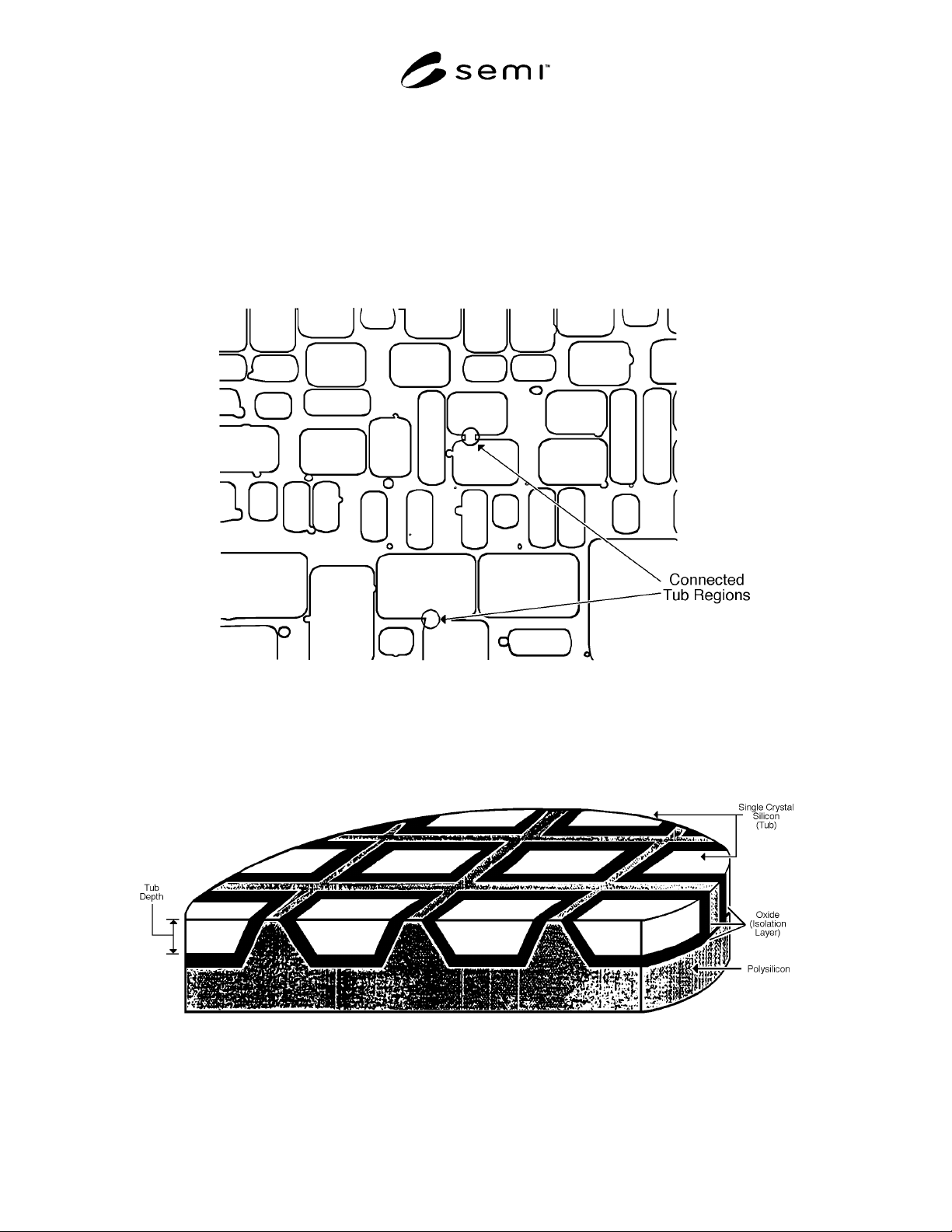
8 Connected
Tubs
None "
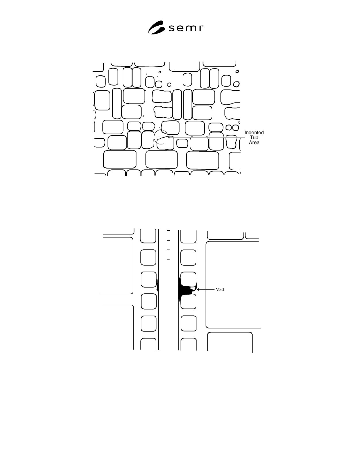
9 Pattern
Deformation
None "
10 Polysilicon
Voids
None "
11 Tub Depth
(> + 5% or
< − 5% from
nominal value)
None "
12 Defective Die 25% 1
Note 1: The number of defects per die is not cumulative; an electrical
die with one or more defects is counted as a single defective die.
7 Test Methods and Measurements
7.1 The supplier and purchaser shall agree in advance
on the means for making all measurements (see Section
9).
7.2 DI Wafer Characteristics
7.2.1 Tub Characteristics — The resistivity,
conductivity, dopant type, and crystal growth method
are difficult to ascertain in the finished DI wafers.
Verification test procedures or certification of these
characteristics shall be agreed upon between the
supplier and the purchaser (see Section 9).
7.2.2 Tub Diffused Layers — The test procedures to
measure the sheet resistance, junction depth, and dopant
type shall be agreed upon between supplier and
purchaser (see Section 9).
7.2.3 Visual Surface Defects and Contamination —
Determine in accordance with ASTM Practice F 523.
7.2.4 Microscopically Observed Die Defects —
Examine a representative sampling of die (see Section
8.2) with an optical microscope with magnification
such that one complete electrical die fills the field of
view. If necessary for verification of defects, move to
higher magnifications as required. Due to the extensive
microscopic inspections required, verification test
procedures or certification of these characteristics shall
be agreed upon between the supplier and the purchaser
(see Section 9).
8 Sampling
8.1 Unless otherwise specified, appropriate sample
sizes shall be selected from each lot according to
ANSI/ASQC Z1.4-1993. Each quality characteristic
shall be an assigned an acceptable quality level (AQL)
in accordance with ANSI/ASQC Z1.4-1993. Inspection
levels shall be agreed upon between supplier and
purchaser.
8.2 The sampling plan for microscopic inspection of
die on the wafer, including number and location of
inspected die, shall be agreed upon between supplier
and purchaser.
9 Certification
9.1 Upon request of the purchaser in the contract or
order, a manufacturer’s or supplier’s certification that
the material was manufactured and tested in accordance
with this specification, together with a report of test
results, shall be furnished at the time of shipment.
9.2 The supplier and purchaser may agree that the
material shall be certified as “capable of meeting”
certain requirements. In this context, “capable of
meeting” shall signify that the supplier is not required
to perform the appropriate tests in Section 7; however,
if the purchaser performs the test and the material fails
to meet the requirement, the material may be subject to
rejection.
10 Packing and Marking
10.1 Special packing requirements shall be subject to
agreement between the supplier and purchaser.
Otherwise all wafers shall be handled, inspected, and
SEMI M22-0303 © SEMI 1992, 2003 4
packed in such a manner to avoid chipping, scratches,
and contamination, and in accordance with the best
industry practices to provide protection against damage
during shipment.
10.2 The wafers supplied under this specification shall
be identified by appropriately labeling the outside of
each box or container and each subdivision thereof in
which it may reasonably be expected that the wafers
will be stored prior to further processing. Identification
shall include supplier’s name and reference no., date,
quantity, DI wafer diameter, DI wafer thickness, and
customer code no. The reference number assigned by
the supplier shall provide ready access to information
concerning the fabrication history of the particular
wafers in that lot. Such information shall be retained on
file at the manufacturer’s facility for at least one year
after the particular lot has been shipped.
Figure 1
Connected Tubs
Figure 2
Cross-Section of DI Wafer
SEMI M22-0303 © SEMI 1992, 2003 5
Figure 3
Pattern Deformation
Figure 4
Void in the Polycrystalline Silicon