semi合集-English.pdf - 第558页
SEMI E78-1102 © SEMI 1998, 2002 16 a charged particle by a char ged surface. This is the only electrostatic effect considered here. For particles of one diameter, d , and one ch arge, q , the particle de position flux, j…
SEMI E78-1102 © SEMI 1998, 2002 15
high current parasitic bipolar action deep in the
substrate and also within the ESD protective structures.
The electrical characteristics found also resistive shorts,
leakages, low breakdown voltages and Icc failures.
R1-1.5.3 CDM ESD Damage
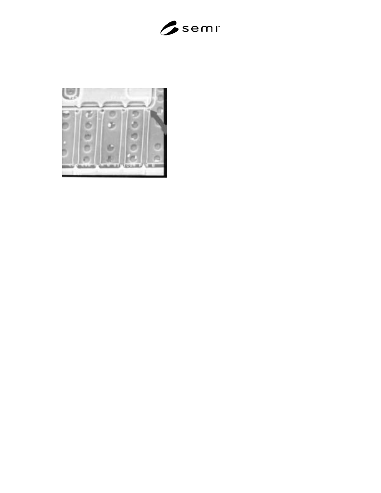
Figure R1-3
Example of CDM Damage
R1-1.5.3.1 In the above CDM example (refer to Figure
R1-3), the gate oxide damage is seen as a unique failure
signature beyond the input protection structures at an
internal location of the die. Most often the oxide failure
is located beneath the poly at the field oxide edge, or is
located at the poly edge adjacent to the source/drain
junction. To date all CDM ESD damage has been found
in the gate oxide at the input buffer circuitry.
R1-1.6 References
Cook, C., Daniel, S., Proceedings EOS/ESD
Symposium, Dallas, TX (1992), p. 149–157
Euzent, B.L., Maloney, T.J., Donner II, J.C.,
Proceedings EOS/ESD Symposium, Las Vegas, NV
(1991), p. 59–64
Morgan, I.H., A Handbook of EOS and ESD Models,
AMD Internal Publication (1992)
Pierce D.G., Shiley, W., Mulcahy, B., Wunder, M.,
Proceedings EOS/ESD Symposium, Anaheim, CA
(1988), p. 137–146
May, J.T., Guravage, J.F., Proceedings ISTFA, Los
Angeles, CA (1990), p. 143–147
Avery, L.R., EOS/ESD Symposium, Orlando, Florida
(1987), p. 186–191
Avery, L.R., Proceedings EOS/ESD Symposium, FL
(1987), p. 88–92
Renninger, R.G., Jon, M.C., Lin, D.L., Diep, T.,
Welsher, T.L., Proceedings EOS/ESD Symposium,
New Orleans, LA (1989), p. 59–71
Bossard, P.R., Chemelli, R.G., Unger, B.A.,
Proceedings EOS/ESD Symposium, San Diego, CA
(1980), p. 17–22
AMD Internal Publications, PLD/CQD EOS/ESD,
EOS/ESD Task Force Reports, July 1993 and January
1994
Raymond, T., Chang, K.L., Henry, Leo G., AMD 3
rd
Engineering Conference, February 1994
ESD STM5.1 — Sensitivity Testing – Human Body
Model (HBM) - Component Level
ANSI/ESD STM5.2 — Sensitivity Testing -- Machine
Model (MM) - Component Level
MIL-STD-883, Method 3015.7, March,1989
Gieser, H.A., Egger, P., Herrmann, M.R., Reiner, J.C.,
Birolini, A., ESREF Proceedings, Bordeaux, France
(1993)
Henry, Leo G., Raymond, T., Mahanpour, M., Morgan,
I., 20th International Symposium for Testing and
Failure Analysis (ISTFA), 1994
R1-2 Enhanced Particle Deposition
Attributable to Electrical Charge on a Wafer
Contributed by Douglas W. Cooper, Ph.D., The
Texwipe Company, Upper Saddle River, NJ 07458.
R1-2.1 Introduction — The presence of excess
electrical charge on a wafer can create an electrostatic
field that will lead to accelerated deposition of particles
onto the wafer. This undesirable consequence is but one
of several threats to product yield posed by the presence
of excess electrical charge on a wafer. Sections R1-1
and R1-3 of this related information discuss two other
important and potentially damaging consequences of
surface charge.
R1-2.1.1 The purpose of the discussion in this section
is to estimate the magnitude of electrostatic field that
can be tolerated before electrostatically enhanced
particle deposition becomes the dominant particle
deposition mechanism. Over the particle size range 0.01
to 0.3 µm, diffusion is the dominant, non-electrostatic
mechanism of particle deposition. Thus, values of
electrostatic fields that do not produce particle
deposition velocities greater than those attributable to
particle diffusion will be deemed tolerable. A set of
such values calculated under a specific and very
restrictive set of conditions are presented in this section.
R1-2.2 Theoretical Background — Although there are
numerous electrostatic interactions between particles
and surfaces, the dominant one is almost always the
“Coulombic” interaction: the attraction (or repulsion) of
SEMI E78-1102 © SEMI 1998, 2002 16
a charged particle by a charged surface. This is the only
electrostatic effect considered here.
For particles of one diameter, d, and one charge, q, the
particle deposition flux, j, (the number of particles
deposited per unit area per unit time) is the product of
aerosol particle number concentration, c; particle
charge, q; the electric field created by the charged
wafer, E; and particle mechanical mobility, B (terminal
velocity per unit external force):
j = cqEB (1
)
The group qEB is the “electrostatic deposition
velocity”, v
elect
v
elect
= qEB =
j
c (2)
The variables q and E are those containing the electrical
parameters that affect the magnitude of v
elect
; B depends
on particle diameter but not electrical properties.
It is the v
elect
values that will be calculated for
comparison with those of v
diff
, the particle deposition
velocity attributable to particle diffusion. Values of E
for which v
elect
< v
diff
will be those deemed tolerable in
wafer manufacturing.
Note that the total number of particles, N, deposited on
a wafer, obtained by integrating Equation (1) over the
wafer area, A, and the time of exposure, t, depends on c
as well as the deposition velocity:
N
= cqEBAt o
r
N
/
A
= ctv
elect
(3)
Reducing c obviously reduces N, but the relative
importance of the differing deposition mechanisms and
the values of the deposition velocities associated with
these mechanisms are assumed to not depend upon c, at
least to a first-order approximation (see, for example,
Peters and Cooper, 1991).
R1-2.2.1 Effect of the Particle Charge, q — There are
many charging and discharging mechanisms for
particles, so q is hard to predict and likely to be highly
variable. In a normal atmosphere the positive and
negative air ions tend to have roughly equal
effectiveness in charging particles, so that the number
of positively charged particles is roughly equal to the
number of negatively charged particles. Thus, about
half the particles will be attracted and half repelled by a
net charge on the wafer. Special circumstances, such as
corona discharge ionizers that are not balanced, could
alter this conclusion. Without ionizers, cleanrooms tend
to have relatively low levels of ions compared to the
outdoor or other indoor atmospheres, because the
HEPA/ULPA filters efficiently remove ions from the
recirculating air.
R1-2.2.1.1 A Boltzmann charge equilibrium, the
charge distribution approximated by aerosol particles
exiting a radioactive neutralizer, is a plausible lower
limit for particle charge and will be assumed in the
calculations of v
elect
, using an improved version of this
distribution developed by Fuchs (1964). Upper limits
on particle charge are determined by ion emission limits
or, in the case of water droplets, the Rayleigh limit.
However, assuming higher particle charge distributions
usually means that v
elect
> v
diff
for virtually any value of
E > 0 and that the only method for avoiding
electrostatically enhanced particle deposition is to
reduce wafer charge to zero. Thus, the Fuchs charge
distribution will be assumed in calculating v
elect
even
though it represents the most favorable particle charge
distribution for minimizing electrostatically enhanced
particle deposition. Under many practical circumstances
the particle charge will be greater and the maximum
tolerable electrostatic field will be lower than that
calculated for the Fuchs charge levels.
R1-2.2.2 The Electrostatic Field, E, Induced by the
Wafer Surface Charge — The electrostatic field will
depend on the charge on the wafer divided by a quantity
with the units of length squared; either a distance
squared (far from the wafer) or an area (close to the
wafer) or some combination at intermediate distances.
While field is not properly measured as a voltage,
measuring the voltage, V, at a fixed distance, s, from the
wafer allows inferring the field from V/s and the
appropriate geometric and dimensional factors. The
electrostatic field to be used in Equation (2) can be
estimated from the ratio of the wafer charge to the
wafer surface area, or the average field near the surface
at the center, E
0
.
R1-2.2.2.1 Very far from the wafer, many wafer
diameters away, the field created by the net wafer
charge, Q, will be similar to that from a point charge:
E
1
= k
1
Qr
2
(4)
where k
1
depends on the system of units used; and r is
the distance from the center of the wafer to the particle.
R1-2.2.2.2 Very close to the wafer, a fraction of a
wafer diameter away, the field created by the net wafer
charge is:
E
2
= k
2
′ Q r
2
(5)
where Q' is the net wafer charge, assumed to be
uniformly distributed, contained within the intersection
of a sphere of radius, r, and centered on the point of the
wafer closest to the particle.
R1-2.2.2.3 This equation indicates that the charge
distribution on the wafer can make a difference close to
the wafer. For an insulating wafer with a uniform
charge and a radius, R:
E
2
= E
0
= k
2
Q
π
R
2
(6)
SEMI E78-1102 © SEMI 1998, 2002 17
at a distance r = R from the center of the wafer.
R1-2.2.2.4 For a conductive wafer, or for a wafer with
localized regions of charge, the electric field will vary
over the surface, causing greater and lesser deposition
velocities. A conductive wafer will have the charge
concentrated near the edges, producing a relatively high
field there and much lower fields as the center is
approached.
R1-2.2.2.5 Note that both E
1
and E
2
are proportional to
Q and therefore, other variables being equal,
electrostatic deposition is expected to be proportional to
Q. Thus, the criterion to be specified is not the tolerable
charge on the wafer but the tolerable electrostatic field
near the wafer surface (such as that evaluated at a
distance of one radius perpendicular to the wafer
surface above its center), E
0
. A maximum tolerable
value of E
0
will be estimated by calculating the
maximum E
0
values for which v
elect
< v
diff
, assuming a
Fuchs distribution for the particle charge.
R1-2.3 Tolerable Electrostatic Field
R1-2.3.1 Particle Deposition Velocity Attributable to
Convective Diffusion (vdiff) — In a microelectronics
cleanroom, airflow is generally laminar
(“unidirectional”) downward at about 50 cm/sec (100
ft/min). If the flow is perpendicular to a surface, such as
a wafer of diameter, Dw, a boundary layer forms across
which particles diffuse to the surface. Liu and Ahn
(1987) adapted the correlation of Sparrow and Geiger
(1985) and obtained a correlation for the average
diffusive deposition velocity as:
v
diff
= 1.08 Sc
13
Re
12
D * D
w
(7)
where Sc =
µ
/
ρ
D * is the Schmidt Number
µ
is the gas viscosity
ρ
is the gas density
and D*= kTB is the particle diffusivity
k is the Boltzmann constant
T is the absolute temperature and
B is the particle mobility
and Re =
ρ
UD
w
/
µ
is the Reynolds number
U is the gas velocity and
D
w
is the wafer diameter
Bae et al. (1994) reviewed the experimental work of
others and presented their own, supporting this
correlation; Cooper et al. (1990) obtained a similar
equation by a somewhat different method. Oh et al.
(1996) summarized prior experimental and theoretical
work and extended the numerical analysis with a
turbulent transport properties model, finding a small
increase in deposition for the conditions modeled.
These authors’ publications support the approximation
that the diffusional deposition velocity is about 0.006
cm/sec at particle diameter of 0.25 µm and about 0.03
cm/sec at particle diameter of 0.01 µm, or:
v
diff
=
(0.03 cm / sec)/(d /0.01
µ
m)
12
(8)
for 0.01 µm ≤ d ≤ 0.3 µm in cleanroom air.
R1-2.3.2 Particle Deposition Velocity Attributable to
Electrostatic Forces (v
elect
) — Using a power law to
approximate the Fuchs particle charge distribution
yields the following approximation for electrical
mobility (Cooper et al., 1990):
Z
=
qB
=
(0.002 cm /
s
)/(d /0.01
µ
m)(1 V / cm) (9)
from which the deposition velocity attributable to
electrostatic forces becomes:
v
elect
=
(0.002 cm
/
s
)[
E
0
/(
V
/
cm)]/(d
/
0.01
µ
m) (10)
Setting v
elect
/v
diff
= 1 results in the following expression
for tolerable E
0
:
[(E
0
/(V /cm)]
=
15 [d /(0.01
µ
m)]
12
(11)
Table R1-2 lists the values of tolerable electrostatic
field adjacent to a wafer surface as calculated from
Equation (11). Note that the electrostatic fields are
calculated at a distance of one wafer radius from the
center of the wafer. E
0
is the value of electric field at
which electrostatically enhanced particle deposition is
estimated to match the particle deposition velocity
attributable to diffusion, assuming a Fuchs charge
distribution on the particles. This charge distribution
represents a minimal particle charge. With most particle
charge distributions to be encountered in practice, even
lower values of electrostatic fields will produce
enhanced deposition. A safe conclusion is that there is
no safe value of electrostatic field that will avoid
enhanced particle deposition unless neutralization of
particle charge has been achieved, in which case the
very modest values of electrostatic fields calculated
from Equation (11) and tabulated in Table Rl-2 should
be tolerable.