semi合集-English.pdf - 第5089页
SEMI M23.3-0600 © SEMI 1994, 2000 3 a b d O. F. I. F. d = 5 mm 10 mm a b O. F. I. F. d d = 5 mm 15 mm Figure A1-2 Rectangular Wafers Which can be Obtained from 50 and 75 mm Round Wafers NOTICE: SEMI makes no w arra nties…
SEMI M23.3-0600 © SEMI 1994, 2000 2
APPENDIX 1
NOTE: The material in this appendix is an official part of SEMI M23.3 and was approved by full letter ballot procedures on
April 21, 2000 by the Japanese Regional Standards Committee.
A1-1 InP is a promising material for photonic devices
such as LDs, LEDs, and photodetectors for fiber
communications. The consumption of InP wafers is
increasing year by year due to the fiber communication
systems such as LAN, ISDN, and others.
A1-2 In order to fabricate these devices, many
rectangular wafers with more than 30 different sizes are
industrially used but most of the sizes are not
reasonably determined. From the viewpoint of material
yield as explained below, the standardization of
rectangular InP wafers is useful not only for InP wafer
manufacturers, but also for device manufacturers.
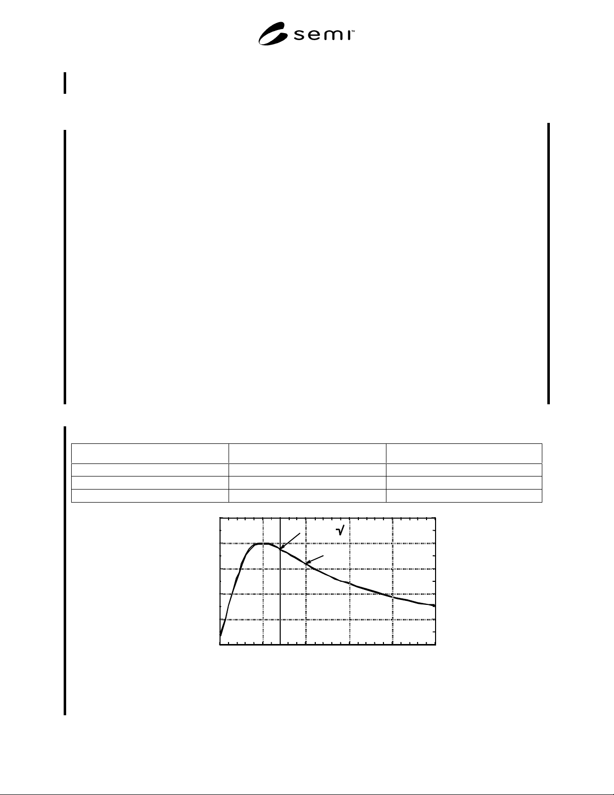
A1-3 Figure A1-1 shows the effective area (A) as a
function of ratio of longitudinal length (a) and of lateral
length (b). It is a fact that the largest area can be
obtained when the shape is square. However, it is
difficult to distinguish V-Groove and Dove-Tail Groove
orientations when the shape is square. It is, therefore,
necessary to make the shape rectangular in a way that
one can distinguish the orientations. It is however,
noted that if the length ratio becomes too large, the
effective area is dramatically decreased as seen in
Figure A1-1. For instance, rectangular wafers at the
point P have very little area, and most of wafer is cut
off in vain. It is, therefore, very reasonable to select the
length ratio at which the effective area is not largely
decreased. When the length ratio (a/b ratio) is √2, the
area decrease is only 5.7% as seen in Table A1-1 and
Figure A1-1. It is also interesting to note that if the
length ratio is determined as √2, each half of the
rectangular wafer again gives a similar shape with the
same ratio. In fact, this length ratio is used for paper
standardization as A3/A4 or B3/B4. Rectangular wafers
are therefore determined SEMI M23.3.
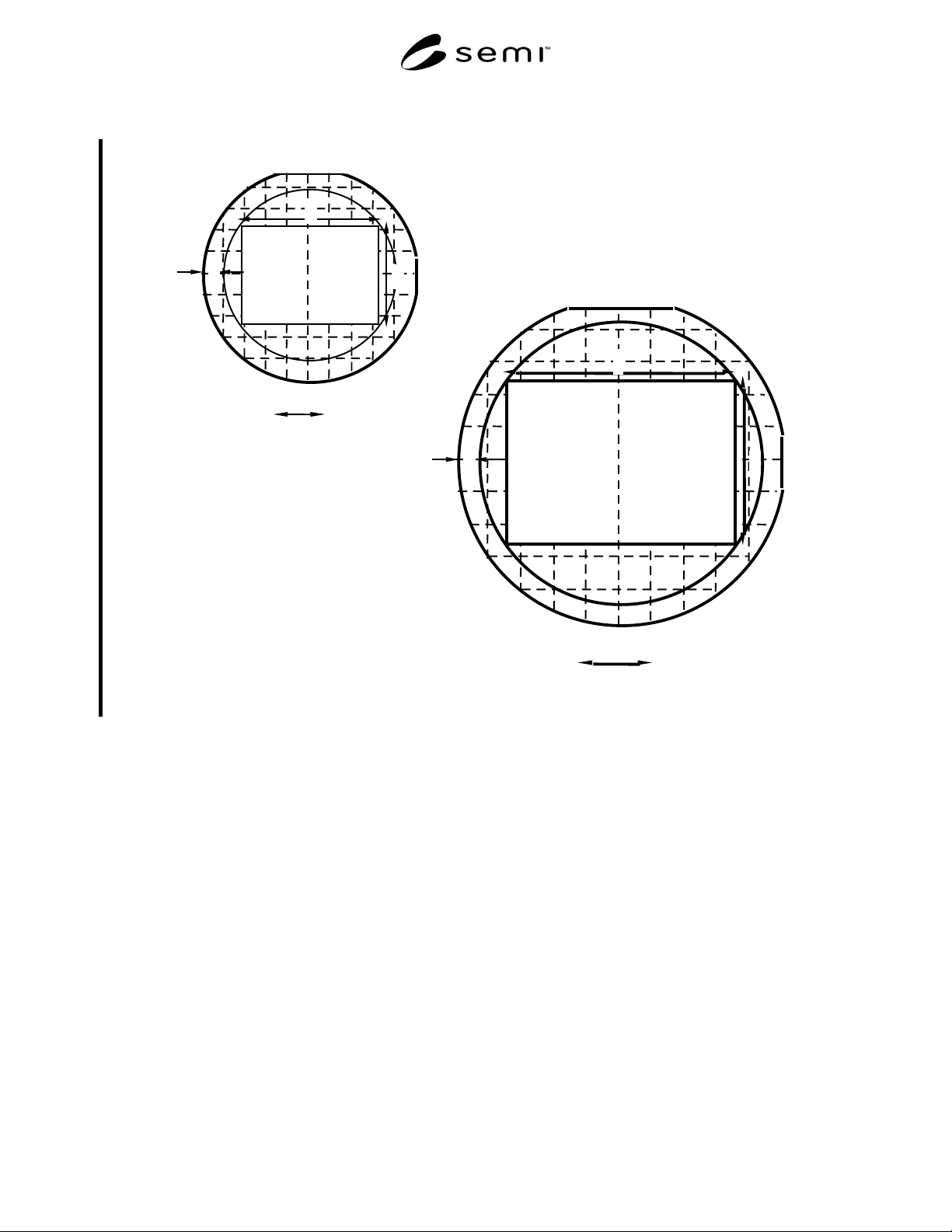
A1-4 Since there are already standardized 50 mm and
75 mm round wafers, the standardization is made in a
way that large rectangular wafers can be obtained from
these standardized wafers by removing 5 mm from the
periphery as seen in Figure A1-2. Removing of 5 mm is
due to EPD measurement specifications in which 5 mm
periphery is excluded from the measurement.
A1-5 As explained above, it is highly recommended to
use the standardized rectangular wafers because this
standardization is very important in preventing
proliferation of various sizes of rectangular wafers in
the future.
Table A1-1
a/b Ratio A (mm
2
) A/square
1.000 800.0 100%
1.414 754.2 94.3%
2.000 640.0 80.0%
543210
0
200
400
600
800
1000
a/bratio
a : b = 2 : 1
P
Effective Area (mm
2
)
Figure A1-1
Effective Area as a Function of a/b Ratio
SEMI M23.3-0600 © SEMI 1994, 20003
a
b
d
O. F.
I. F.
d = 5 mm
10 mm
a
b
O. F.
I. F.
d
d = 5 mm
15 mm
Figure A1-2
Rectangular Wafers Which can be Obtained from 50 and 75 mm Round Wafers
NOTICE: SEMI makes no warranties or representations as to the suitability of the standard set forth herein for any
particular application. The determination of the suitability of the standard is solely the responsibility of the user.
Users are cautioned to refer to manufacturer’s instructions, product labels, product data sheets, and other relevant
literature respecting any materials mentioned herein. These standards are subject to change without notice.
The user’s attention is called to the possibility that compliance with this standard may require use of copyrighted
material or of an invention covered by patent rights. By publication of this standard, SEMI takes no position
respecting the validity of any patent rights or copyrights asserted in connection with any item mentioned in this
standard. Users of this standard are expressly advised that determination of any such patent rights or copyrights, and
the risk of infringement of such rights, are entirely their own responsibility.
Copyright by SEMI® (Semiconductor Equipment and Materials
International), 3081 Zanker Road, San Jose, CA 95134. Reproduction o
f
the contents in whole or in part is forbidden without express written
consent of SEMI.
SEMI M23.4-0999 © SEMI 19991
SEMI M23.4-0999
SPECIFICATION FOR ROUND 100 mm POLISHED
MONOCRYSTALLINE INDIUM PHOSPHIDE WAFERS FOR
ELECTRONIC AND OPTOELECTRONIC DEVICE APPLICATIONS
(DOVE-TAIL TYPE)
This specification was technically approved by the Global Compound Semiconductor Committee and is the
direct responsibility of the Japanese Compound Semiconductor Committee. Current edition approved by the
Japanese Regional Standards Committee on June 1, 1999. Initially available at www.semi.org August 1999;
to be published September 1999.
NOTE: The complete specification for this product includes all general requirements of SEMI M23.
Table 1 Dimension and Tolerance Requirements
Property Dimension Tolerance Units
DIAMETER (See NOTE 1.) 100.0 ± 0.5 mm
THICKNESS, CENTER POINT 625.0 ± 25 µm
PRIMARY FLAT LENGTH 32.5 ± 2 mm
SECONDARY FLAT LENGTH 18.0 ± 2 mm
NOTE 1: The diameter standard means that the dimension is centered to this value.
Table 2 Orientation and Flat Location Requirements
Property Requirement
OPTION Dove-Tail
PRIMARY FLAT ORIENTATION
) 1 1 (0 ± 0.5 (see Figure 1 in SEMI M23) under an indium facet. The primary
flat shall be perpendicular to the “Dove-Tail” etch figure (see NOTE 1).
SECONDARY FLAT ORIENTATION
) 1 1 0( 90°=± 5° clockwise from the primary flat.
SURFACE ORIENTATION
A.
(100) ± 0.5°=(See Figure 1 in SEMI M23.)
B.
(100) off 2° ± 0.5° toward the
0) 1 (1 plane (see NOTE 2).
(See Figure 2 in SEMI M23.)
ORTHOGONAL MISORIENTATION
± 5°=(See Figure 3 in SEMI M23.)
NOTE 1: Since there are various etchants, the appropriate etching method for revealing etch pits can be determined by each manufacturer. For
example, see reference “HBr-K
2
Cr
2
O
7
-H
2
O etching system for indium phosphide” J.L. Weyher et al., Materials Science and Engineering, B28
(1994) 488-492.
NOTE 2: The frame of reference is the (100) plane of the crystal. It is the wafer normal that is tilted toward the
0) 1 (1 plane of the crystal.
NOTICE: SEMI makes no warranties or representations as to the suitability of the standards set forth herein for
any particular application. The determination of the suitability of the standard is solely the responsibility of the user.
Users are cautioned to refer to manufacturer’s instructions, product labels, product data sheets, and other relevant
literature respecting any materials mentioned herein. These standards are subject to change without notice.
The user’s attention is called to the possibility that compliance with this standard may require use of copyrighted
material or of an invention covered by patent rights. By publication of this standard, SEMI takes no position
respecting the validity of any patent rights or copyrights asserted in connection with any item mentioned in this
standard. Users of this standard are expressly advised that determination of any such patent rights or copyrights, and
the risk of infringement of such rights, are entirely their own responsibility.
Copyright by SEMI® (Semiconductor Equipment and Materials
International), 3081 Zanker Road, San Jose, CA 95134. Reproduction o
f
the contents in whole or in part is forbidden without express written
consent of SEMI.