semi合集-English.pdf - 第7236页
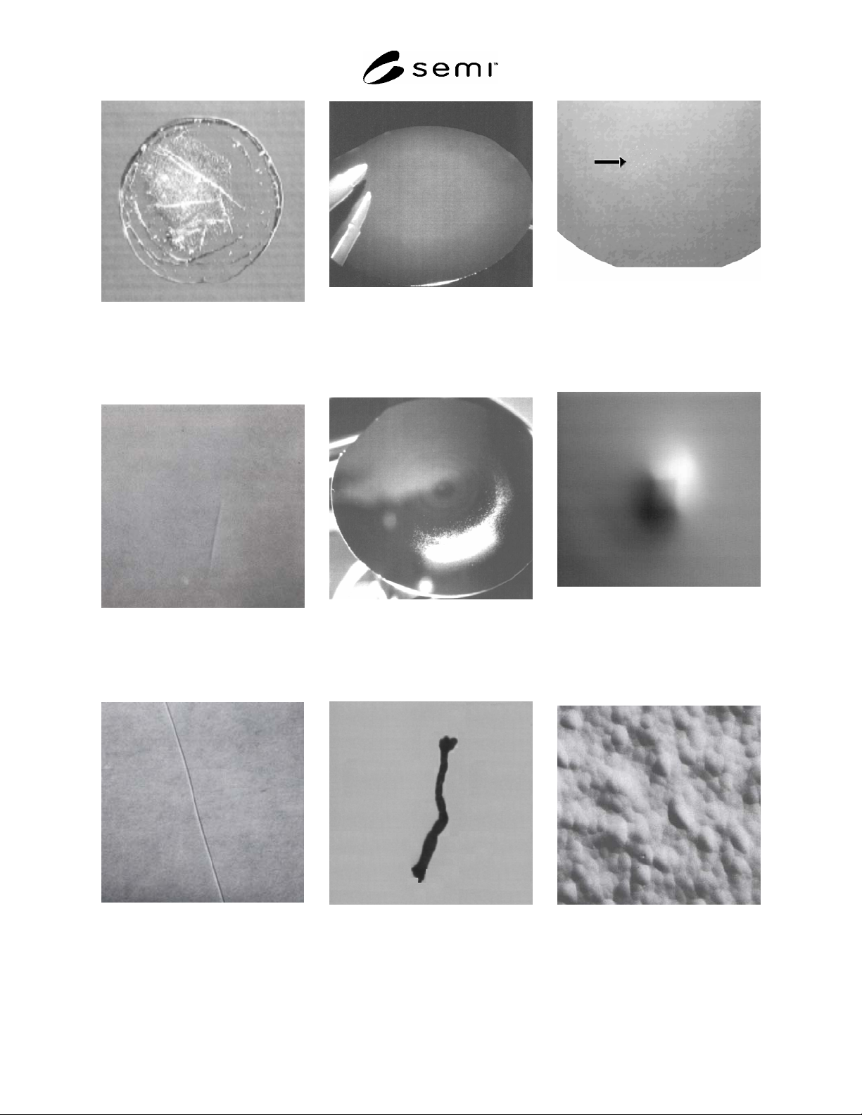
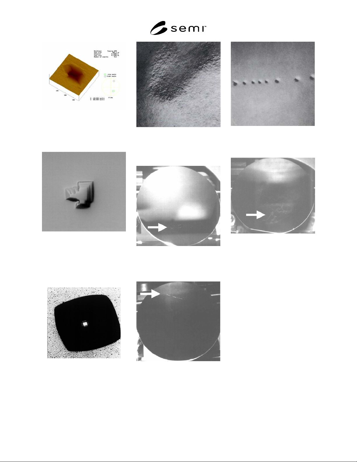
SEMI MF154-0305 © SEMI 2003, 2005 10 Figure 61 Atomic Force Microscope (AF M) Image of a Faceted COP Figure 62 Pit (Usually Associated With Insufficient Polishing of Caustic Etched Wafer), Magnificati on 1000× NOTE: Air …
SEMI MF154-0305 © SEMI 2003, 2005 9
Figure 52
Foreign Matter from a Dried
Liquid Spot, Magnification 200×
Figure 53
Groove or Micro-Scratch,
Magnification 220×
Figure 54
Groove or Micro-Scratch,
Magnification 220×
Figure 55
Haze Seen as Distortion or
Blurring of a Reflected Image,
Full Wafer View
Figure 56
Haze (Extreme Case) Seen as a
White Cloudiness Under High
Intensity Light, Full Wafer View
Figure 57
Localized Light Scatterers,
(Particle Contamination) in the
Form of Small Fiber,
Magnification 200×
Figure 58
Localized Light Scatterers Seen
in High Intensity Light, Full
Wafer View
Figure 59
Mound, No Preparation
Required, Magnification 200×
Figure 60
Orange Peel Surface Roughness,
Magnification 200×
SEMI MF154-0305 © SEMI 2003, 2005 10
Figure 61
Atomic Force Microscope (AFM)
Image of a Faceted COP
Figure 62
Pit (Usually Associated With
Insufficient Polishing of Caustic
Etched Wafer),
Magnification 1000×
NOTE: Air Pocket Size Ranges from a
Few Micrometers to a Few Hundred
Micrometers
Figure 63
Pit Associated with a Crystal Air
Pocket on Lapped Wafer
Figure 64
Saw Blade Defect Seen on
Lapped and Etched Wafer,
Magnification 6×
Figure 65
Multiple Scratches Located by
the Arrow under High Intensity
Light, Full Wafer View
Figure 66
A Single Long Arc Scratch
Located by the Arrow
Under High Intensity Light,
Full Wafer View
Figure 67
Scratch Resulting in a Series of
Pits Following Chemical Etching,
Magnification 70×
Figure 68
Stains from Improper Cleaning
or Drying Located by the Arrow
under High Intensity Light,
Full Wafer View

SEMI MF154-0305 © SEMI 2003, 2005 11
NOTICE: SEMI makes no warranties or representations as to the suitability of the standards set forth herein for any
particular application. The determination of the suitability of the standard is solely the responsibility of the user.
Users are cautioned to refer to manufacturer's instructions, product labels, product data sheets, and other relevant
literature, respecting any materials or equipment mentioned herein. These standards are subject to change without
notice.
By publication of this standard, Semiconductor Equipment and Materials International (SEMI) takes no position
respecting the validity of any patent rights or copyrights asserted in connection with any items mentioned in this
standard. Users of this standard are expressly advised that determination of any such patent rights or copyrights, and
the risk of infringement of such rights are entirely their own responsibility.
Copyright by SEMI® (Semiconductor Equipment and Materials
International), 3081 Zanker Road, San Jose, CA 95134. Reproduction of
the contents in whole or in part is forbidden without express written
consent of SEMI.