semi合集-English.pdf - 第4888页
SEMI M3-0304 © SEMI 1978, 2004 8 RELATED INFORMATION 1 RECOMMENDED SAPPHIRE SUBSTR ATE FRONT SURFACE DEFECT LIMITS NOTICE : This related information is not an official part of SEMI M3 and was derived fr om the original e…
SEMI M3-0304 © SEMI 1978, 2004 7
APPENDIX 1
SPECIFICATION FOR 3 INCH RECLAIMED SAPPHIRE SUBSTRATES
NOTICE: The material in this appendix is an official part of SEMI M3 and was approved by full letter ballot
procedures on September 3, 2003. The material in this appendix was originally included in SEMI M3.6-88,
Standard for 3 inch Reclaimed Sapphire Substrates.
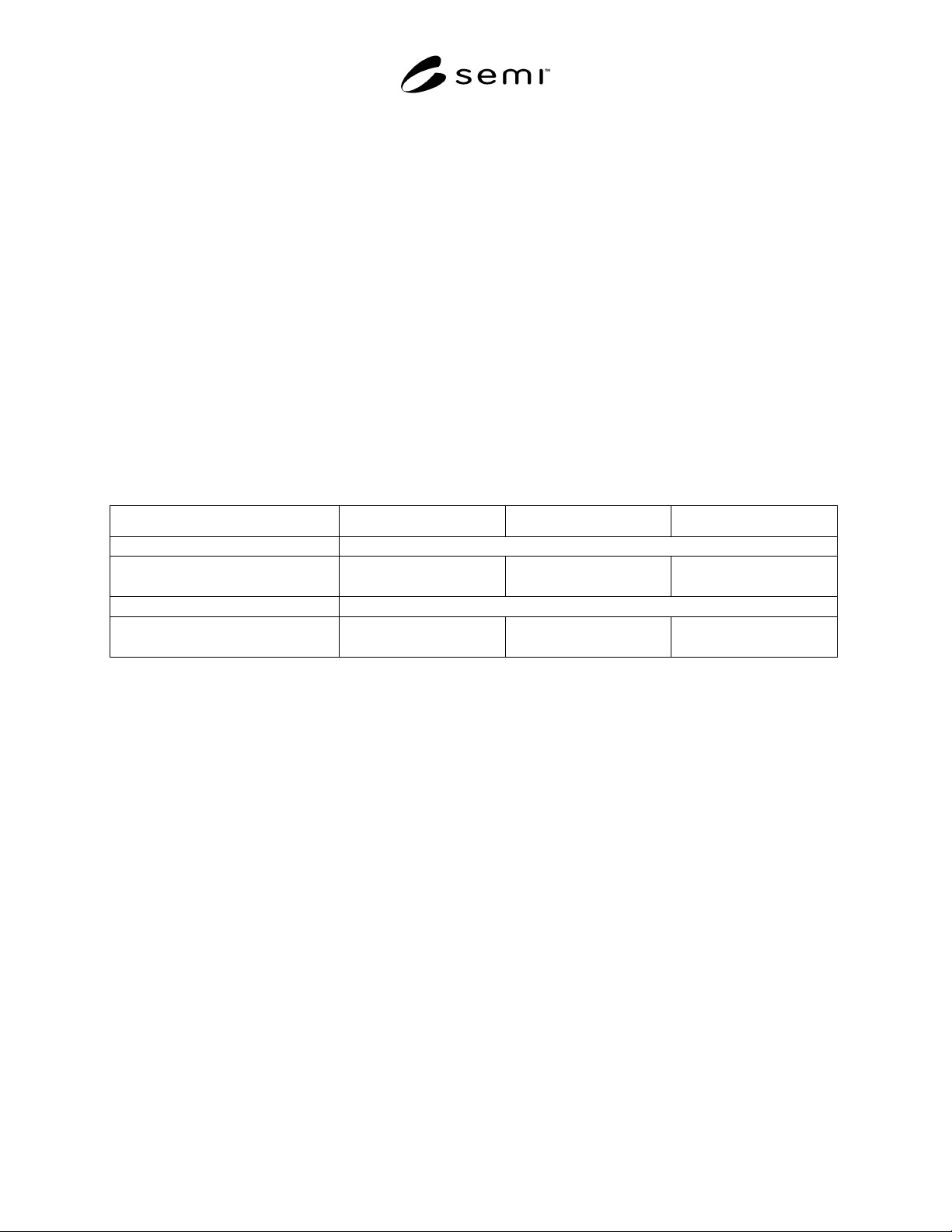
A1-1.1 Dimensional specifications for 3 inch reclaimed sapphire substrates are given in Table A1-1.
A1-1.2 Surface orientation shall be as received for reclamation.
A1-1.3 Flat location(s) shall be as received for reclamation.
A1-1.4 Flatness shall be classified in accordance with Table 2. The amount of surface damage and flatness of the
as-received substrate determines final flatness.
A1-1.5 Front surface finish shall be in accordance with the purchase order or contract. See Related Information 2
for recommendations on acceptable front surface finish level.
A1-1.6 Back surface finish shall be as received for reclamation.
A1-1.7 Other characteristics, including sampling, test methods, surface defect limits, certification, and packing and
marking, shall be as specified in SEMI M3.
Table A1-1 Dimensional Specification
Property Min Max Units (see NOTE 1)
DIAMETER As received for reclamation.
THICKNESS, CENTER POINT
(see NOTE 2)
0.014
360
0.019
480
in.
µm
FLAT LENGTH As received for reclamation.
BOW, max 0.002
51
in.
µm
NOTE 1: For referee purposes, the U.S. Customary units apply. Conversion to metric (SI) equivalents was done following the maximum-
minimum convention in which the minimum values are rounded up and the maximum values are rounded down to ensure that the equivalent
range is always inside the referee range. If the metric equivalents are used for incoming inspection measurements, the rightmost digit of
minimum values should be reduced by 1 and the rightmost digit of maximum values should be increased by 1 to avoid rejection of material that is
within the specification when measured by the referee system of units. CAUTION — The significance of the rightmost digit may vary,
depending on the quantity being measured and the precision of the test procedure. Refer to the relevant test method for precision data that can be
used to construct appropriate guard bands.
NOTE 2: Amount of surface damage and flatness of as-received substrate determines final substrate thickness.

SEMI M3-0304 © SEMI 1978, 2004 8
RELATED INFORMATION 1
RECOMMENDED SAPPHIRE SUBSTRATE FRONT SURFACE DEFECT
LIMITS
NOTICE: This related information is not an official part of SEMI M3 and was derived from the original edition of
the specifications which erroneously included this optional material as a part of the text of the specification. This
related information was approved for publication by full letter ballot procedure on September 3, 2003.
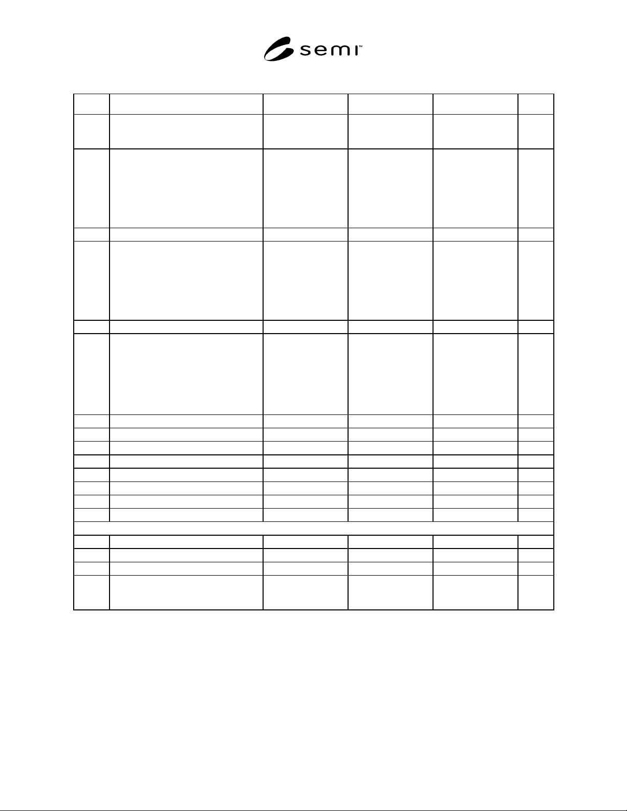
R1-1 Definitions for surface defects are found in SEMI MF523, where defects commonly found on silicon slices are
defined. Some of these terms do not apply to sapphire substrates, but are present in Table R-1, which lists
recommended limits for front surface defect levels, to provide a convenient reference point to the silicon wafer
standards, such as SEMI M1.
R1-1.1 Minimal Conditions and/or Dimensions — Minimal conditions or dimensions for defects are stated below
and shall be used for determining substrate acceptability unless other minimal limiters are agreed upon by the
interested parties. Anomalies less than these limits shall not be considered defects.
R1-1.2 Area Contamination — Foreign matter on the surface in localized areas which is revealed as discolored,
mottled, or cloudy appearance resulting from smudges, stains, water spots, etc.
R1-1.3 Contamination — Any foreign matter detectable under the inspection lighting conditions.
R1-1.4 Edge Chips and Indents — Any edge or surface anomaly conforming to the accepted definition greater than
0.010 inch in radial depth and peripheral length.
R1-1.5 Cracks — Any anomaly conforming to the accepted definition greater than 0.010 inch (0.25 mm) in total
length.
R1-1.6 Craters — Any individually distinguishable surface anomaly conforming to the accepted definition visible
when viewed under diffuse illumination.
R1-1.7 Crow’s Feet — N.A.
R1-1.8 Grooves — N.A.
R1-1.9 Haze — Haze is indicated when the image of a narrow beam tungsten lamp filament is detectable on the epi
silicon surface. (Under some conditions, contamination may appear as haze.)
R1-1.10 Mounds — N.A.
R1-1.11 Orange Peel — Any visually detectable roughened surface conforming to the accepted definition
observable under diffuse illumination.
R1-1.12 Pits — Any individually distinguishable nonremovable surface anomaly conforming to the accepted
definition visible when viewed under intense illumination.
R1-1.13 Saw Exit Mark — N.A.
R1-1.14 Scratch — Any anomaly conforming to the definition with a length-to-width ratio greater than 5:1.
R1-1.15 Striation — Any feature conforming to the accepted definition detectable under background lighting
conditions.
SEMI M3-0304 © SEMI 1978, 2004 9
Table R1-1 Recommended Sapphire Substrate Defect Limits
Item Characteristics Max Defect Limit AQL (see NOTE 6) Illumination Notes
1 SCRATCHES
Maximum Number
Maximum Length
3
R/2
High Intensity 1
2 PITS
Maximum Number
2" Diameter Substrate
3" Diameter Substrate
100 mm Diameter Substrate
125 mm Diameter Substrate
150 mm Diameter Substrate
4
9
15
20
25
4% Cum. 1, 2
3 HAZE None — see NOTE 4 4% Cum. 4
4 CONTAMINATION/PARTICULATE
Maximum Number
2" Diameter Substrate
3" Diameter Substrate
100 mm Diameter Substrate
125 mm Diameter Substrate
150 mm Diameter Substrate
4
9
15
20
25
4% Cum. Diffuse 1, 2
5 CONTAMINATION/AREA None
6 EDGE CHIPS
Maximum Number
Maximum Radial Penetration
Maximum Single Chip
Peripheral Length
Maximum Cumulative
Peripheral Length
see NOTE 3
2
0.12" (3 mm)
0.250" (6.35 mm)
0.250" (6.35 mm)
4% Cum. Diffuse 3
7 CRACKS, CROW' S FEET see NOTE 6 6
8 CRATERS None 1, 5
9 DIMPLES None 1
10 GROOVES None 4% Cum. 1, 5
11 MOUNDS None 1, 5
12 ORANGE PEEL None Diffuse 1
13 SAW MARKS None 1, 5
14 STRIATIONS
SLICE BACK SURFACE
15 CHIPS see NOTE 3 see NOTE 3 Diffuse 3
16 CRACKS, CROW' S FEET None see Note 6 6
17 CONTAMINATION/AREA None
18 SAW MARKS
Incidence
Maximum Depth
N.A. see Note 5 5
NOTE 1: The outer 4 mm annulus is excluded from these criteria.
NOTE 2: Ninety percent of substrate shall be free of contaminants after pre-inspection treatment. Balance of substrate may have light-reflecting
particles up to the limit established for Item 2 — Pits.
NOTE 3: All chips shall be beveled. Chips less than 0.4 mm should not be counted.
NOTE 4: Haze refers to epitaxial silicon appearance only, not to condition of polished sapphire substrate.
NOTE 5: These defects are not observed in SOS wafers. Terms remain for convenient reference to silicon specification.
NOTE 6: Cracks are observed in sapphire substrates as fractures or as surface separations along cleavage planes. The cumulative AQL for both
front surface and back surface of substrate is 4% for both. Crow’s feet see Note 5.